R8C/1A Group, R8C/1B Group 19. Electrical Characteristics
Rev.1.30 Dec 08, 2006 Page 295 of 315
REJ09B0252-0130
i = 0 or 1
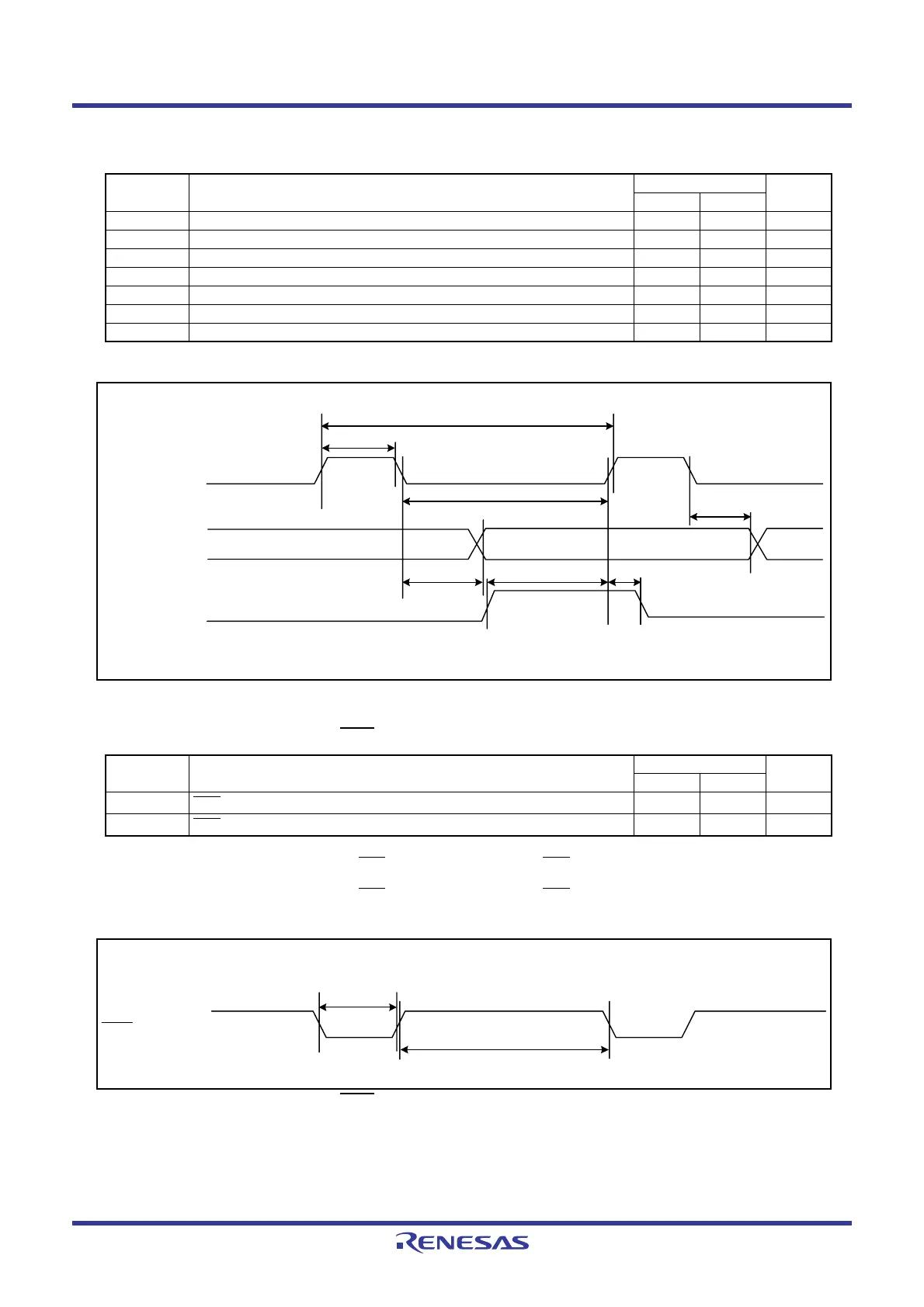
Figure 19.16 Serial Interface Timing Diagram when VCC = 3 V
NOTES:
1. When selecting the digital filter by the INT0
input filter select bit, use an INT0 input HIGH width of either (1/digital filter clock
frequency x 3) or the minimum value of standard, whichever is greater
2. When selecting the digital filter by the INT0
input filter select bit, use an INT0 input LOW width of either (1/digital filter clock
frequency x 3) or the minimum value of standard, whichever is greater
Figure 19.17 External Interrupt INT0 Input Timing Diagram when VCC = 3 V
Table 19.26 Serial Interface
Symbol Parameter
Standard
Unit
Min. Max.
t
c(CK) CLKi input cycle time 300 − ns
t
W(CKH) CLKi input “H” width 150 − ns
t
W(CKL) CLKi input “L” width 150 − ns
t
d(C-Q) TXDi output delay time − 80 ns
t
h(C-Q) TXDi hold time 0 − ns
t
su(D-C) RXDi input setup time 70 − ns
t
h(C-D) RXDi input hold time 90 − ns
Table 19.27 External Interrupt INT0 Input
Symbol Parameter
Standard
Unit
Min. Max.
t
W(INH)
INT0 input “H” width
380
(1)
− ns
t
W(INL)
INT0 input “L” width
380
(2)
− ns
tW(CKH)
tc(CK)
tW(CKL)
th(C-Q)
th(C-D)
tsu(D-C)td(C-Q)
CLKi
TXDi
RXDi
VCC = 3 V
i = 0 or 1
INT0 input
t
W(INL)
tW(INH)
VCC = 3 V
 Loading...


