R8C/1A Group, R8C/1B Group 7. Voltage Detection Circuit
Rev.1.30 Dec 08, 2006 Page 46 of 315
REJ09B0252-0130
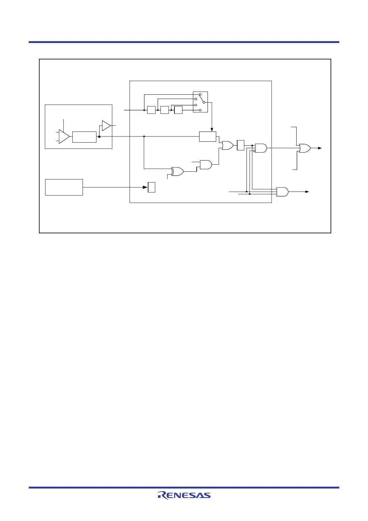
Figure 7.3 Block Diagram of Voltage Monitor 2 Interrupt / Reset Generation Circuit
+
-
1/2 1/2 1/2
Voltage detection 2 circuit
VCA27
VCC
Internal
reference
voltage
VCA13
Noise filter
(Filter width: 200 ns)
Voltage detection 2 signal
is held “H” when VCA27 bit
is set to 0 (disabled).
Voltage
detection
2 signal
Digital
Filter
fRING-S
VW2F1 to VW2F0
= 00b
= 01b
= 10b
= 11b
VW2C1
VW2C2 bit is set to 0 (not detected)
by writing 0 by a program.
When VCA27 bit is set to 0 (voltage
detection 2 circuit disabled), VW2C2
bit is set to 0.
VW2C2
VW2C7
VW2C3
Watchdog timer block
Watchdog timer
underflow signal
This bit is set to 0 (not detected) by writing
0 by a program.
VW2C0
VW2C6
Non-maskable
interrupt signal
Voltage monitor 2
interrupt signal
Watchdog
timer interrupt
signal
Oscillation stop
detection
interrupt signal
Voltage monitor 2 interrupt/reset generation circuit
VW2C0 to VW2C3, VW2F2, VW2F1, VW2C6, VW2C7: Bits in VW2C register
VCA13: Bit in VCA1 register
VCA27: Bit in VCA2 register
Voltage
monitor 2
reset signal
 Loading...


