R8C/1A Group, R8C/1B Group 10. Clock Generation Circuit
Rev.1.30 Dec 08, 2006 Page 75 of 315
REJ09B0252-0130
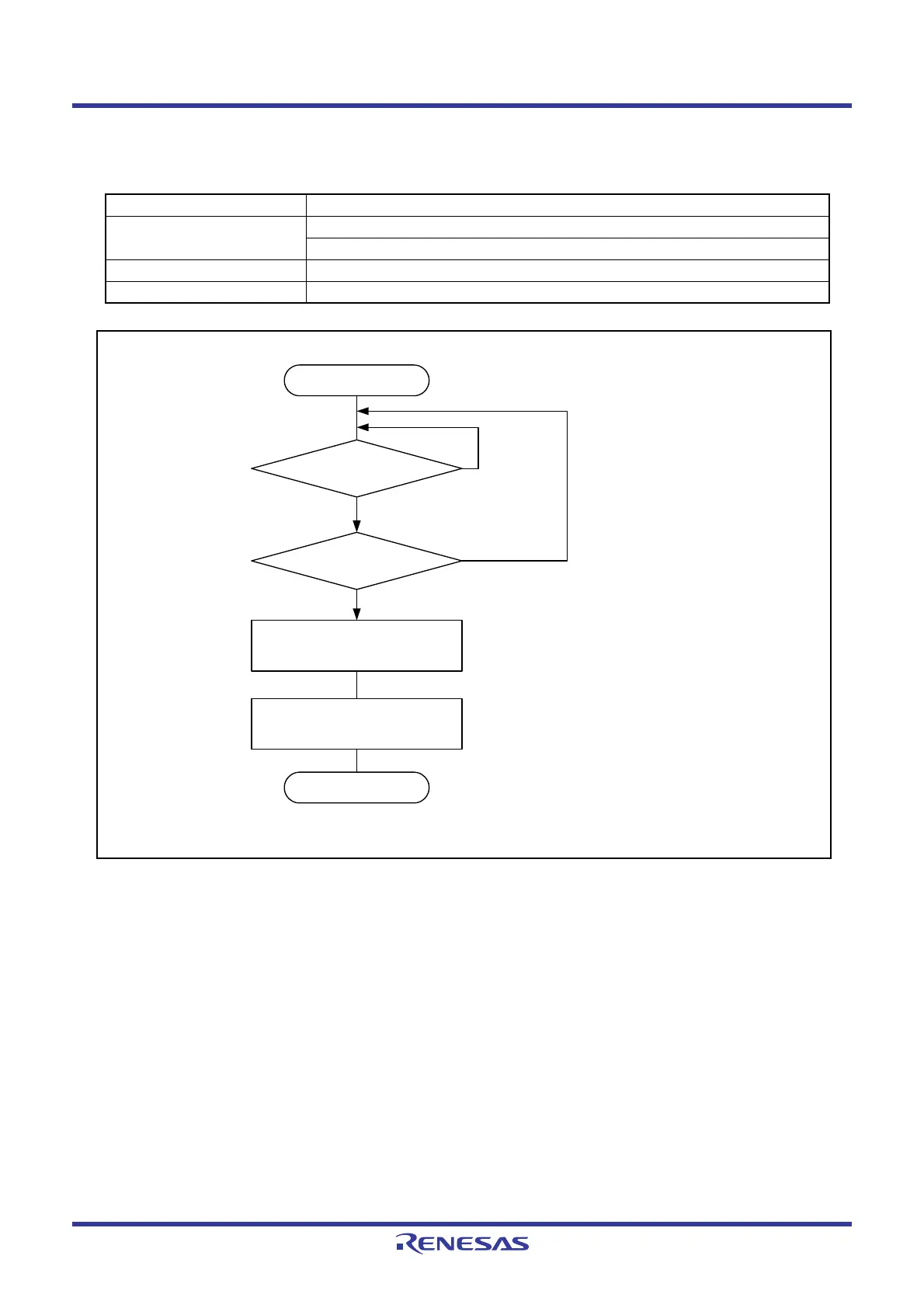
Figure 10.11 Procedure for Switching Clock Source from Low-Speed On-Chip Oscillator to Main
Clock
Table 10.6 Determining Interrupt Source for Oscillation Stop Detection, Watchdog Timer, and
Voltage Monitor 2 Interrupts
Generated Interrupt Source Bit Showing Interrupt Cause
Oscillation stop detection
( (a) or (b) )
(a) OCD3 bit in OCD register = 1
(b) Bits OCD1 to OCD0 in OCD register = 11b and OCD2 bit = 1
Watchdog timer VW2C3 bit in VW2C register = 1
Voltage monitor 2 VW2C2 bit in VW2C register = 1
Determine OCD3 bit
1(main clock stops)
0 (main clock oscillates)
Set bits OCD1 to OCD0 to 00b
(oscillation stop detection function
disabled)
Set OCD2 bit to 0
(select main clock)
End
Switch to main clock
Bits OCD3 to OCD0: Bits in OCD register
Judge several times
Determine several times that the main clock is supplied
 Loading...


