Table of contents
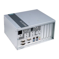
SIMATIC IPC PX-39A
8 Operating Instructions, 08/2022, A5E51699601-AA
10 Standards and approvals ................................................................................................................... 102
10.1 Scope .............................................................................................................................. 102
10.2 CE marking ...................................................................................................................... 102
10.3 UKCA marking ................................................................................................................. 103
10.4 DIN ISO 9001 certificate and software license agreements................................................ 103
10.5 UL approval ..................................................................................................................... 103
10.6 FCC (USA) ........................................................................................................................ 104
10.7 Canada ............................................................................................................................ 104
10.8 Australia / New Zealand ................................................................................................... 104
10.9 Eurasion Customs Union EAC ........................................................................................... 105
10.10 Korea .............................................................................................................................. 105
10.11 Taiwan ............................................................................................................................ 105
A Hardware description ........................................................................................................................ 106
A.1 Motherboard ................................................................................................................... 106
A.1.1 Layout of the motherboard .............................................................................................. 106
A.1.2 Position of the interfaces on the motherboard .................................................................. 107
A.2 Internal interfaces ............................................................................................................ 108
A.2.1 Pin assignment of the internal interfaces .......................................................................... 108
A.2.2 USB ports ......................................................................................................................... 108
A.3 Bus board ........................................................................................................................ 109
A.3.1 Slot for expansion cards on the bus board ........................................................................ 109
A.3.2 Pin assignment power supply connection for expansion cards .......................................... 109
A.4 External interfaces ........................................................................................................... 110
A.5 System resources ............................................................................................................. 111
A.5.1 Currently allocated system resources ............................................................................... 111
A.5.2 I/O address allocation ....................................................................................................... 111
A.5.2.1 Overview of the internal module registers ........................................................................ 111
A.5.2.2 Battery status register (read only) .................................................................................... 112
A.5.2.3 Watchdog timer (WDT) register (read/write) ..................................................................... 113
A.5.2.4 NVRAM address register ................................................................................................... 114
B Technical support .............................................................................................................................. 115
B.1 Service and support ......................................................................................................... 115
B.2 Troubleshooting .............................................................................................................. 116
B.2.1 Problems with device functions ........................................................................................ 116
B.2.2 Problems when booting the device .................................................................................. 117
B.2.3 Problems when using expansion cards ............................................................................. 117
 Loading...