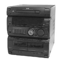
HCD-J3MD
4949
Waveforms
– BD ( CD) SECTION –
– BD (MD) (1/2) SECTION –
– BD (MD) (2/2) SECTION –
– MAIN (3/3) Section –
• Indication of transistor
THIS NOTE IS COMMON FOR PRINTED WIRING
BOARDS AND SCHEMATIC DIAGRAMS.
(In addition to this, the necessary note is printed in
each block.)
Note on Schematic Diagram:
• All capacitors are in µF unless otherwise noted. pF: µµF
50 WV or less are not indicated except for electrolytics
and tantalums.
• All resistors are in Ω and
1
/
4
W or less unless otherwise
specified.
•
f
: internal component.
• C : panel designation.
• U : B+ Line.
• V : B– Line.
• H : adjustment for repair.
• Voltages and waveforms are dc with respect to ground in
service mode.
• Voltages are taken with a VOM (Input impedance 10 MΩ).
Voltage variations may be noted due to normal production
tolerances.
• Waveforms are taken with a oscilloscope.
Voltage variations may be noted due to normal production
tolerances.
• no mark : STOP
( ) : PLAY
< > : REC
∗
: can not be measured.
• Circled numbers refer to waveforms.
• Signal path.
F : FM
d : PB (TAPE)
G : REC (TAPE)
J : CD
c : CD (digital out)
E : PB (MD)
j : REC (MD)
p : PB (digital out)
l : REC (digital in)
Note on Printed Wiring Board:
• X : parts extracted from the component side.
• x : parts mounted on the conductor side.
•
a
: Through hole.
• b : Pattern from the side which enables seeing.
Q
C
EB
These are omitted.
CEB
These are omitted.
IC101 #ª (FE)
1
2
3
4
IC101 yh XTAI
IC101 ta (RF AC)
IC101 $¡ (FE)
IC101 @§ (MDP)
5
3.1Vp-p
16.9MHz
1.2Vp-p
(PLAY)
2.5V
APPROX 500mVp-p
7.5µsec
2.4Vp-p
1
2
3
IC101 1, 2 (I, J) (PLAY mode)
IC101 4 (A) (PLAY mode)
IC101 8, 9 (E, F) (PLAY mode)
0.46Vp-p
0.1Vp-p
0.06Vp-p
4
5
6
7
8
IC121 !§ (OSCI)
IC121 @¶ (LRCK)
IC121 @ª (FS256)
IC121 @• (XBCK)
IC121 (º (FS4)
3.1Vp-p
22.581MHz
3.2Vp-p
44.1kHz
3.8Vp-p
2.822MHz
3.8Vp-p
11.29MHz
3.2Vp-p
176.4kHz
1
2
IC501 !¡ XC-OUT
IC501 !£ X-OUT
32.768kHz
5.2Vp-p
16MHz
5.5Vp-p
IC316 !£ (XOUT)
1
3.2Vp-p
10MHz
– MD DIGITAL Section –
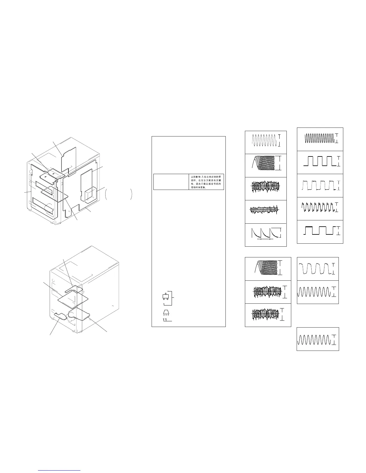
6-2. CIRCUIT BOARDS LOCATION
PANEL board
TUNER unit
AMP board
MAIN board
MD DIGITAL board
TRANS board
TC board
Entire tuner unit is
suppliled as a single
complete tuner block.
LOADING board
BD (CD) boar
BD (MD) board
SW board
The components identified by
mark 0 or dotted line with mark
0 are critical for safety.
Replace only with part number
specified.