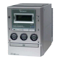
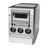
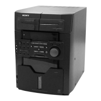
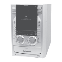
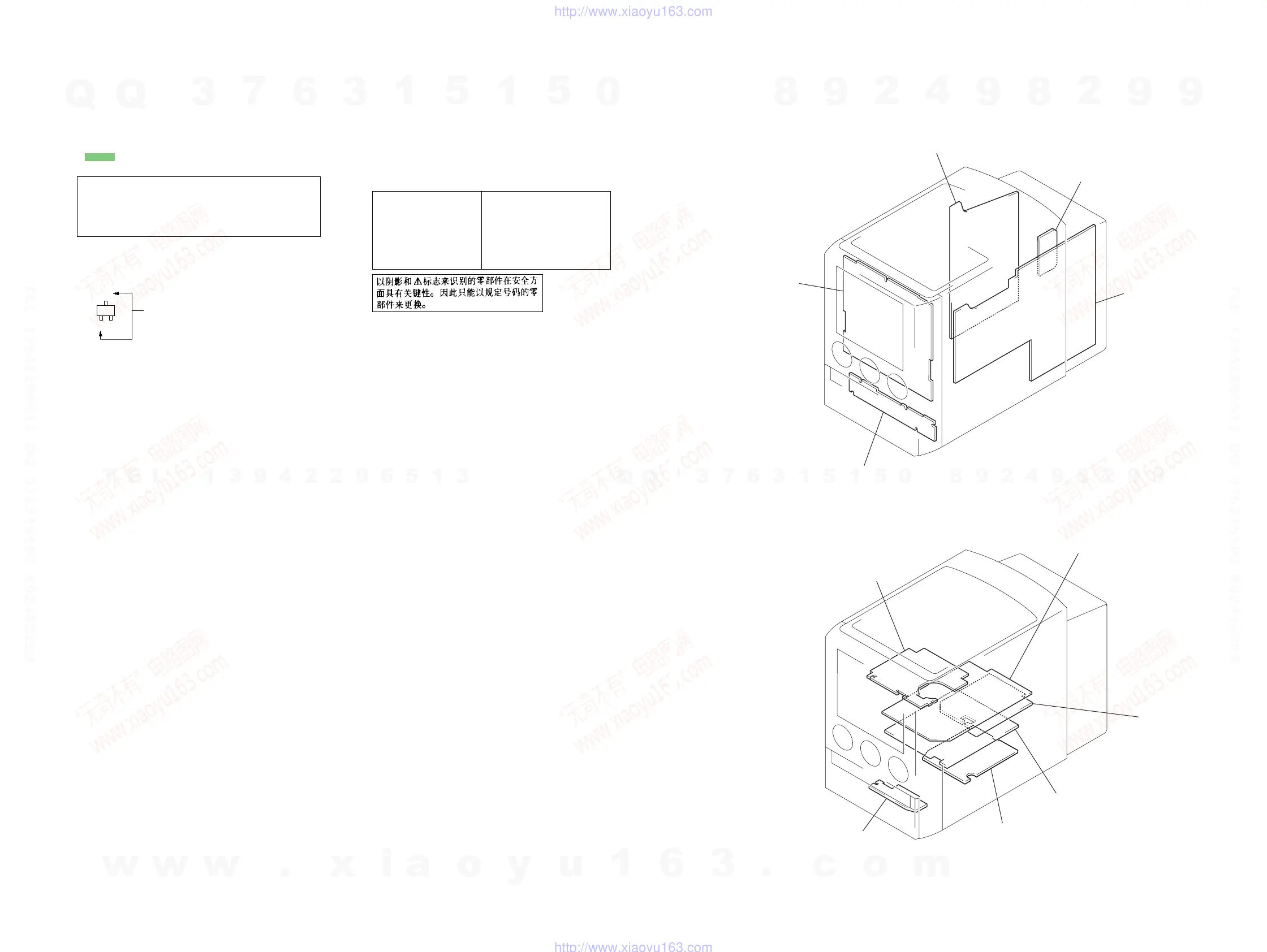
HCD-M90
3535
TC board
CONTROL board
RF-240 board
DAC board
DVD board
LOADING board
Note:
The components identi-
fied by mark 0 or dotted
line with mark 0 are criti-
cal for safety.
Replace only with part
number specified.
Note:
Les composants identifiés par
une marque 0 sont critiques
pour la sécurité.
Ne les remplacer que par une
pièce portant le numéro
spécifié.
6-7. NOTE FOR PRINTED WIRING BOARDS AND SCHEMATIC DIAGRAMS
Note on Printed Wiring Boards:
• X : parts extracted from the component side.
• Y : parts extracted from the conductor side.
• W : indicates side identified with part number.
•
f
: internal component.
• : Pattern from the side which enables seeing.
(The other layers' patterns are not indicated.)
Note on Schematic Diagram:
• All capacitors are in µF unless otherwise noted. pF: µµF
50 WV or less are not indicated except for electrolytics
and tantalums.
• All resistors are in Ω and
1
/
4
W or less unless otherwise
specified.
•
f
: internal component.
• C : panel designation.
• A : B+ Line.
• B : B– Line.
• H : adjustment for repair.
•Voltages are taken with a VOM (Input impedance 10 MΩ).
Voltage variations may be noted due to normal produc-
tion tolerances.
•Waveforms are taken with a oscilloscope.
Voltage variations may be noted due to normal produc-
tion tolerances.
• Circled numbers refer to waveforms.
• Signal path.
f : TUNER (FM/AM)
E : TAPE PLAY
a : REC
c : DVD PLAY
J : CD PLAY
F : DVD/CD PLAY (AUDIO)
L : DVD/CD PLAY (VIDEO)
g : DVD/CD PLAY (DIGITAL OUT)
j : MD (VIDEO)
•Abbreviation
AUS: Australian model
CH : Chinese model
CND : Canadian model
SP : Singapore model
C
B
These are omitted.
E
Q
• Circuit Boards Location
Caution:
Pattern face side: Parts on the pattern face side seen from
(Side B) the pattern face are indicated.
Parts face side: Parts on the parts face side seen from
(Side A) the parts face are indicated.
•DVD board is multi-layer board.
However, the patterns of intermediate-layer not been included in
diagram.
• Indication of transistor.
JACK board
SWITCH board
POWER board
VIDEO board
MAIN board
Ver 1.3
w
w
w
.
x
i
a
o
y
u
1
6
3
.
c
o
m
Q
Q
3
7
6
3
1
5
1
5
0
9
9
2
8
9
4
2
9
8
T
E
L
1
3
9
4
2
2
9
6
5
1
3
9
9
2
8
9
4
2
9
8
0
5
1
5
1
3
6
7
3
Q
Q
TEL 13942296513 QQ 376315150 892498299
TEL 13942296513 QQ 376315150 892498299
http://www.xiaoyu163.com
http://www.xiaoyu163.com