96
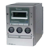
HCD-M90
• CONTROL BOARD IC306 M30620MCN-A11FP (SYSTEM CONTROLLER)
Pin No. Pin Name I/O Description
1
DAC RESET O Reset signal output to the D/A converter “L”: reset
2
RDS DATA I
Serial data input from the RDS decoder (at tuner function)
(RDS decoder is used for the AEP and UK models)
3
LCD RS O Reset signal output to the liquid crystal display “L”: reset
4
SIRCS
I
Sircs remote control signal input
5
LCD DATA O Serial data output to the liquid crystal display
6
LCD STB O Strobe signal output to the liquid crystal display
7
LCD SCK O Serial data transfer clock signal output to the liquid crystal display
8
BYTE — Not used
9
CNVSS — Not used
10
XCIN I Sub system clock input terminal (32.768 kHz)
11
XCOUT O Sub system clock output terminal (32.768 kHz)
12
RESET I
System reset signal input “L”: reset
For several hundreds msec. after the power supply rises, “L”: is input, then it changes to “H”
13
XOUT O Main system clock output terminal (16 MHz)
14
VSS — Ground terminal
15 XIN
IMain system clock input terminal (16 MHz)
16
VCC — Power supply terminal (+4V)
17
NMI I Not used (pull up)
18
RDS-INT I
Serial data transfer clock signal input from the RDS decoder
(RDS decoder is used for the AEP and UK models)
19
SYSCS I Chip select signal input from the DVD system controller
20
AC-CUT I AC cut signal input “L”: AC cut on
21
ST MUTE O Muting on/off control signal output terminal Not used
22
ST CE
O
Chip enable signal output to the tuner unit
23
ST DOUT
O
Serial data output to the tuner unit
24
PWM3
O
Power on/off control signal output terminal Not used
25
ST DIN
I
PLL serial data input from the tuner unit
26
PWM2
O
Power on/off control signal output terminal Not used
27
ST CLK O Serial data transfer clock signal output to the tuner unit (at tuner function)
28
PWM1
O
Power on/off control signal output terminal Not used
29
IIC-CLK O IIC data transfer clock signal output terminal Not used
30
IIC-DATA O IIC data output terminal Not used
31
TXD1 O Serial data output terminal Not used
32
RXD1 I Serial data input terminal Not used
33
SCLK O Video muting control signal output to the video buffer
34
PLL-LOCK DET
I PLL lock detect signal input
35
DATA
O
Serial data output to the DVD system controller
36
XLT
I
Serial data input from the DVD system controller
37
CLK I Serial data transfer clock signal input from the DVD system controller
38 PLAY SW I
Head position detect switch input terminal “L”: forward direction, “H”: reverse direction
39
LINE MUTE O
Line muting on/off control signal output to the recording/playback equalizer amp
“H”: muting on
40
TUNER ON O
Power supply on/off control signal output for the tuner section (+9.5V)
“H”: tuner power on
w
w
w
.
x
i
a
o
y
u
1
6
3
.
c
o
m
Q
Q
3
7
6
3
1
5
1
5
0
9
9
2
8
9
4
2
9
8
T
E
L
1
3
9
4
2
2
9
6
5
1
3
9
9
2
8
9
4
2
9
8
0
5
1
5
1
3
6
7
3
Q
Q
TEL 13942296513 QQ 376315150 892498299
TEL 13942296513 QQ 376315150 892498299
http://www.xiaoyu163.com
http://www.xiaoyu163.com