98
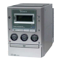
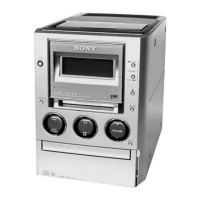
HCD-M90
Pin No. Pin Name I/O Description
84 STK PWR O
Power on/off control signal output to the power amp “L”: power on
85
H/P MUTE O Muting on/off control signal output terminal Not used
86
AMP CE
O
Chip enable signal output to the electrical volume
87
VOL-SDA O Serial data output to the electrical volume
88
AMP CLK O Serial data transfer clock signal output to the electrical volume
89 STK MUTE O
Muting on/off control signal output to the power amp “H”: muting on
90
END SW
I
Tape end detect switch input terminal “H” input when the tape end detected
91
TC SW I Half detect (side A and B) switch and cassette in detect switch input terminal (A/D input)
92
MODEL IN I Destination setting terminal
93
SPEC IN I Destination setting terminal
94, 95
KEY1, KEY2 I Key input terminal (A/D input)
96
AG — Not used
97
KEY3 I Key input terminal (A/D input)
98
VREF O Reference voltage (+4V) input terminal (for A/D conversion)
99
AVCC — Power supply terminal (+4V)
100
DC DETECT I Protect on/off control signal input from the speaker protect circuit “L”: protect on
w
w
w
.
x
i
a
o
y
u
1
6
3
.
c
o
m
Q
Q
3
7
6
3
1
5
1
5
0
9
9
2
8
9
4
2
9
8
T
E
L
1
3
9
4
2
2
9
6
5
1
3
9
9
2
8
9
4
2
9
8
0
5
1
5
1
3
6
7
3
Q
Q
TEL 13942296513 QQ 376315150 892498299
TEL 13942296513 QQ 376315150 892498299
http://www.xiaoyu163.com
http://www.xiaoyu163.com