54
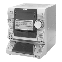
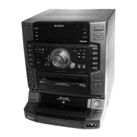
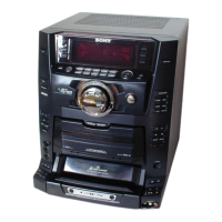
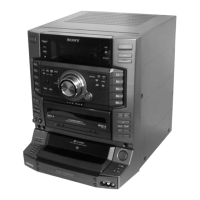
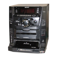
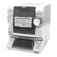
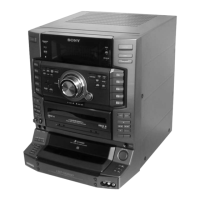
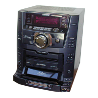
HCD-XG60/XG500
Pin No. Pin Name I/O Description
43
GR-1
O
Grid drive signal output to the fluorescent indicator tube (FL601)
44 to 66 SEG-1 to SEG-23 O
Segment drive signal output to the fluorescent indicator tube (FL601)
67 LED STANDBY O
LED drive signal output of the I/1 indicator (D601) “H”: LED on
68 VKK —
Power supply terminal (–35V) (for fluorescent indicator tube drive)
69 VDD —
Power supply terminal (+5V)
70 XIN I
System clock input terminal (12.5 MHz)
71 VSS —
Ground terminal
72 XOUT O
System clock output terminal (12.5 MHz)
73 RESET I
System reset signal input from the reset signal generator (IC801) “L”: reset
For several hundreds msec. after the power supply rises, “L” is input, then it changes to “H”
74 JOG A I
Jog dial pulse input from the rotary encoder (S763 JOG DIAL) (A phase input)
75 JOG B I
Jog dial pulse input from the rotary encoder (S763 JOG DIAL) (B phase input)
76 TEST I
Connected to ground
77 ——
Not used (open)
78 I2C DATA I/O
Communication data bus with the system controller (IC501)
79 I2C CLK I/O
Communication data reading clock signal input or transfer clock signal output with the system
controller (IC501)
80 D-SW I
CD door open/close detection switch (S742) input terminal “L”: close, “H”: open

 Loading...