50
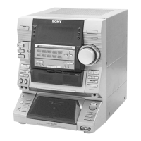
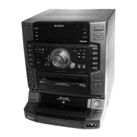
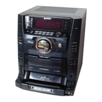
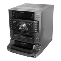
HCD-XG60/XG500
7-30. IC PIN FUNCTION DESCRIPTION
• MAIN BOARD IC501 M30622MAA-A92FP (SYSTEM CONTROLLER (CD MECHANISM CONTROL))
Pin No. Pin Name I/O Description
1 STK-POWER O
Power amplifier on/off selection signal output “L”: standby mode, “H”: power amplifier on
2 POWER O
Power on/off control signal output for the audio system (+5V) and deck, panel, audio system
(+7V) and FM/AM tuner unit (+10V) “L”: standby mode, “H”: power on
3 F-RELAY O
Relay drive signal output for the front speaker protect “H”: relay on
4 REAR-RELAY O
Relay drive signal output for the rear speaker protect “H”: relay on Not used (open)
5 CD-POWER O
Power on/off control signal output for the CD mechanism deck section
“L”: standby mode, “H”: power on
6 LINE-MUTE O
Line muting on/off control signal output “L”: muting on, “H”: muting off
7 DBFB-H/L O
DBFB normal/high selection signal output to the M62493FP (IC101)
“L”: DBFB high, “H”: DBFB low (normal)
8, 9 — —
Connect to ground
10 XC-IN I
Sub system clock input terminal (32.768 kHz)
11 XC-OUT O
Sub system clock output terminal (32.768 kHz)
12 RESET I
System reset signal input from the reset signal generator (IC801) “L”: reset
For several hundreds msec. after the power supply rises, “L” is input, then it changes to “H”
13 X-OUT O
Main system clock output terminal (16 MHz)
14 VSS —
Ground terminal
15 X-IN I
Main system clock input terminal (16 MHz)
16 VDD —
Power supply terminal (+5V)
17
NMI
I
Non-maskable interrupt input terminal Fixed at “H” in this set
18 WAKE UP I
Wakeup control signal input from the fluorescent indicator tube driver (IC601) “L” active
19 SCOR
I Subcode sync (S0+S1) detection signal input from the CXD2587Q (IC101)
20 RDS-INT I
Serial data transfer clock signal input from the RDS decoder on the FM/AM tuner unit
(Used for the AEP and UK models)
21 RDS-DATA I
Serial data input from the RDS decoder on the FM/AM tuner unit
(Used for the AEP and UK models)
22 AC-CUT I
AC off detection signal input from the reset signal generator (IC801) “L”: AC cut checked
23 PL-CLK O
Serial data transfer clock signal output to the pro-logic circuit Not used (open)
24 PL-DATA O
Serial data output to the pro-logic circuit Not used (open)
25 PL-LAT O
Serial data latch pulse output to the pro-logic circuit Not used (open)
26 TIMER LED O
LED drive signal output terminal Not used (open)
27 PROTECT I
Protect on/off detection signal input from the speaker protect circuit
“L”: protect on, “H”: protect off
28
V MUTE
O
Video muting on/off control signal output to the BA7615N (IC191)
“L”: muting off, “H”: muting on
29 IIC-CLK I/O
Communication data reading clock signal input or transfer clock signal output with the fluorescen
indicator tube driver (IC601)
30 IIC-DATA I/O
Communication data bus with the fluorescent indicator tube driver (IC601)
31 NO-USE O
Not used (open)
32
SQ-DATA
I
Subcode Q data input from the CXD2587Q (IC101)
33
SQ-CLK
I
Subcode Q data reading clock signal output to the CXD2587Q (IC101)
34 SW-MODE O
Music/movie mode selection signal output to the M62493FP (IC101)
“L”: movie mode , “H”: music mode
35
CD-DATA
O
Serial data output to the CXD2587Q (IC101)
36 H/P IN I
Connection detection signal input of the headphone jack (J803)
“L”: no connected, “H”: headphone connected
37 CD-CLK O
Serial data transfer clock signal output to the CXD2587Q (IC101)
38 493-LAT O
Serial data latch pulse output to the M62493FP (IC101)

 Loading...