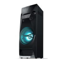
MHC-V6D
76
Pin No. Pin Name I/O Description
110
TEST-MON4/
SD_D0_0
O Software checking signal output terminal for the test port Not used
111
ANALOG-CSEL/
SD_D1_0
O Digital audio signal selection signal output terminal
112
RGB-TRANS-LED-
SPK/SD_WP_0
O LED drive transfer signal output terminal Not used
113
RGB-TRANS-LED/
SD_CD_0
O LED drive transfer signal output to the LED driver
114 ST-RDS I RDS interrupt signal input from the tuner unit
115 ST-CE O Power on/off control signal output to the tuner unit
116 VSS - Ground terminal
117 PCONT-DAMP O Power on/off control signal output to the switching regulator “H”: power on
118 RGB-PWM-CLK O Serial data transfer clock signal output to the LED driver
119 VCC - Power supply terminal (+1.2V)
120 /AMP-RESET O
Reset signal output terminal “L”: reset
Fan motor drive signal output terminal
121 VSS - Ground terminal
122 CD-MOTOR+ O Loading motor drive signal output to the optical pick-up block (forward direction)
123 PVCC - Power supply terminal (+3.3V)
124 CD-MOTOR– O Loading motor drive signal output to the optical pick-up block (reverse direction)
125 CP-CLK O Serial data transfer clock output to the EEPROM
126 CP-DATA I/O Two-way serial data with the EEPROM
127 ST-CLK O Serial data transfer clock signal output to the tuner unit
128 ST-DATA I/O Two-way serial data with the tuner unit
129 NFC-IRQ I Interrupt request signal input from the NFC
130 /PS-PROTECT I Power supply protect signal input terminal
131 /AMP-SD I Shutdown signal input terminal
132 /DC-DET I Speaker DC detection signal input terminal
133 BT-TXD O Transmit data output to the Bluetooth module
134 FL-BK O Latch signal output to the fl uorescent indicator tube
135 SIRCS I SIRCS signal input from remote control receiver
136 AMP-CLK-FR O Amplifi er clock signal output terminal
137 RGB-SCLK O Serial data transfer clock signal output to the LED driver
138 VSS - Ground terminal
139 USB-X1 I USB clock input terminal Not used
140 USB-X2 O USB clock output terminal Not used
141 USBDPVCC - Power supply terminal (+3.3V)
142 USBDPVSS - Ground terminal
143, 144 DM1, DP1 I/O Not used
145 VBUSIN1 I Not used
146 USBDVCC - Power supply terminal (+1.2V)
147 USBDVSS - Ground terminal
148 USBDPVCC - Power supply terminal (+3.3V)
149 USBDPVSS - Ground terminal
150, 151 DM0, DP0 I/O Not used
152 VBUSIN0 I Not used
153 USBDVCC - Power supply terminal (+1.2V)
154 USBDVSS - Ground terminal
155 REFIN I USB reference power supply input terminal
156 USBAPVSS - Ground terminal
157 USBAPVCC - Power supply terminal (+3.3V)
158 USBAVCC - Power supply terminal (+1.2V)
159 USBAVSS - Ground terminal
160 USBUVCC - Power supply terminal (+1.2V)
161 USBUVSS - Ground terminal
162, 163 VSS - Ground terminal
164 MTK-POWER-CTRL O Power on/off control signal output terminal for CD section “H”: power on
165 C-CONT O Charging control signal output terminal
166, 167
Q-Flash-SIO2,
Q-Flash-SIO3
I/O Two-way serial data with to the serial fl ash
168 Q-Flash-CLK O Serial data transfer clock signal output to the serial fl ash

 Loading...