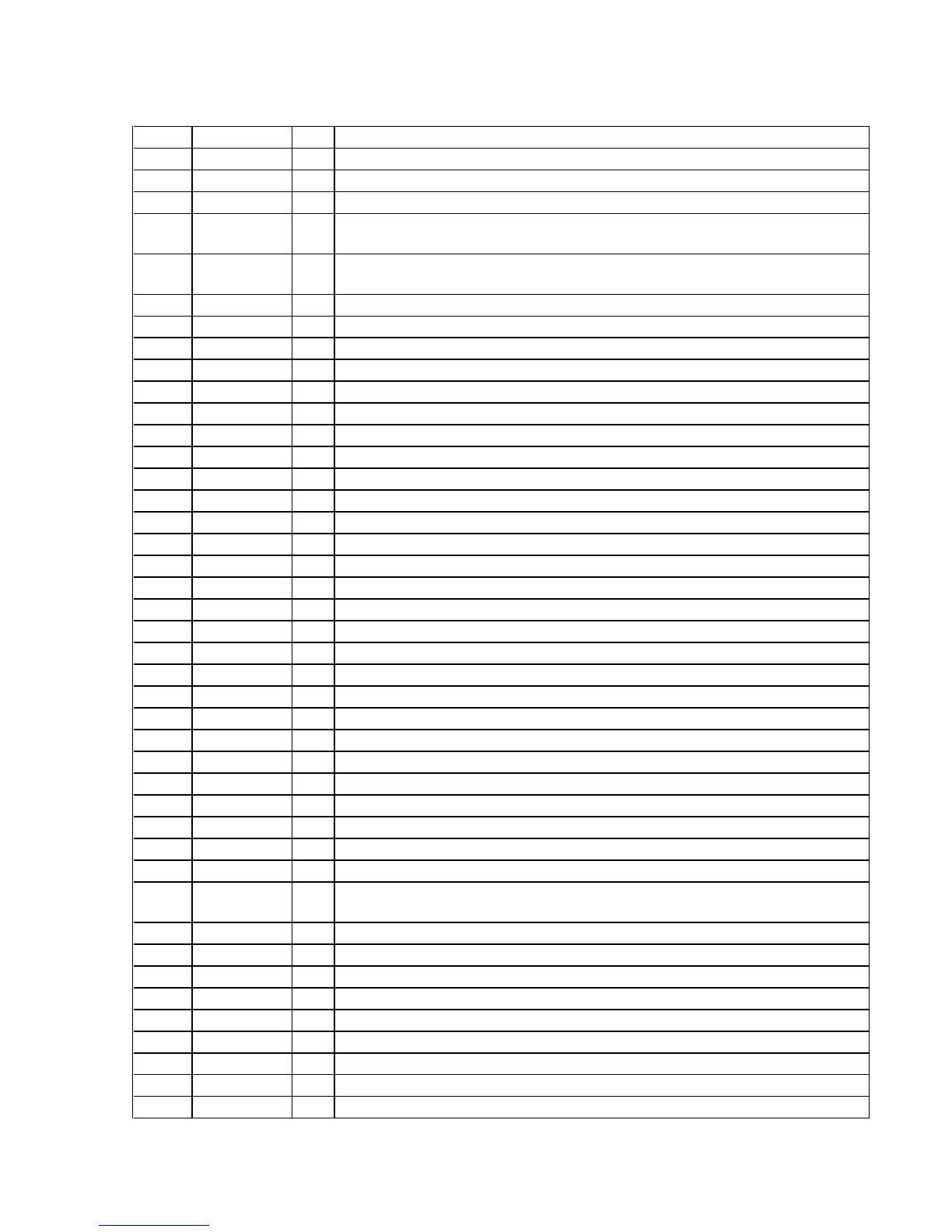
95
STR-DA5000ES
• DIGITAL BOARD IC2251 CXD9616BR (DIGITAL SIGNAL PROCESSOR)
Pin No. Pin Name I/O Description
1
VDDI —
Power supply terminal (+2.5V)
2
EXTIN I
Master clock signal input terminal Not used
3, 4
WMD1, WMD0 I
External memory wait mode setting terminal Fixed at “H” in this set
5MOD1I
Operation mode setting terminal “L”: enhanced mode, “H”: normal mode
Fixed at “H” in this set
6
MOD0 I
Operation mode setting terminal “L”: single chip mode, “H”: can not use
Fixed at “L” in this set
7
VSS —
Ground terminal
8XRST I
System reset signal input from the main system controller “L”: reset
9
VSS —
Ground terminal
10
SCKOUT O
Internal serial clock signal output terminal Not used
11
VDDI (PLL) —
Power supply terminal (+2.5V) (for PLL)
12
SYNC I
Sync/non-sync setting terminal “L”: sync, “H”: non-sync Fixed at “H” in this set
13 to 15
PAGE2 to PAGE0
O
External memory page selection signal output terminal Not used
16 PLOCK O
Internal PLL lock signal output terminal Not used
17
BTACK I
Boot mode state display signal output terminal Not used
18
VDDE —
Power supply terminal (+3.3V)
19
VSS —
Ground terminal
20 to 22
D31 to D29 I/O
Two-way data bus with the S-RAM
23 A17 O
Address signal output terminal Not used
24
VSS —
Ground terminal
25
SDO3 O
Audio serial data output to the lip sync adjust
26
SDO4 O
Audio serial data output to the lip sync adjust
27, 28
SDI1, SDI2 I
Audio serial data input from the digital signal processor
29
LRCKI1 I
L/R sampling clock signal (44.1 kHz) input from the digital signal processor
30
VSS —
Ground terminal
31, 32
D28, D27 I/O
Two-way data bus with the S-RAM
33
A16 O
Address signal output terminal Not used
34
A15 O
Address signal output to the S-RAM
35
SDI3 I
Audio serial date input from the digital signal processor
36
L2 —
Not used
37
VDDI —
Power supply terminal (+2.5V)
38
BCKI1 I
Bit clock signal (2.8224 MHz) input from the digital signal processor
39
SDI4 I
Audio serial data input from the digital signal processor
40
MS I
Master/slave setting terminal “L”: internal clock, “H”: external clock
Fixed at “L” in this set
41, 42
A14, A13 O
Address signal output to the S-RAM
43, 44
D26, D25 I/O
Two-way data bus with the S-RAM
45
VSS —
Ground terminal
46
BCKI2 I
Bit clock signal (2.8224 MHz) input terminal Not used
47, 48
FS2, FS1 I
Sampling frequency selection signal input terminal Not used
49
SPDIF I
SPDIF signal input terminal Not used
50
A12 O
Address signal output to the S-RAM
51 to 53
D24 to D22 I/O
Two-way data bus with the S-RAM
54
VDDE —
Power supply terminal (+3.3V)