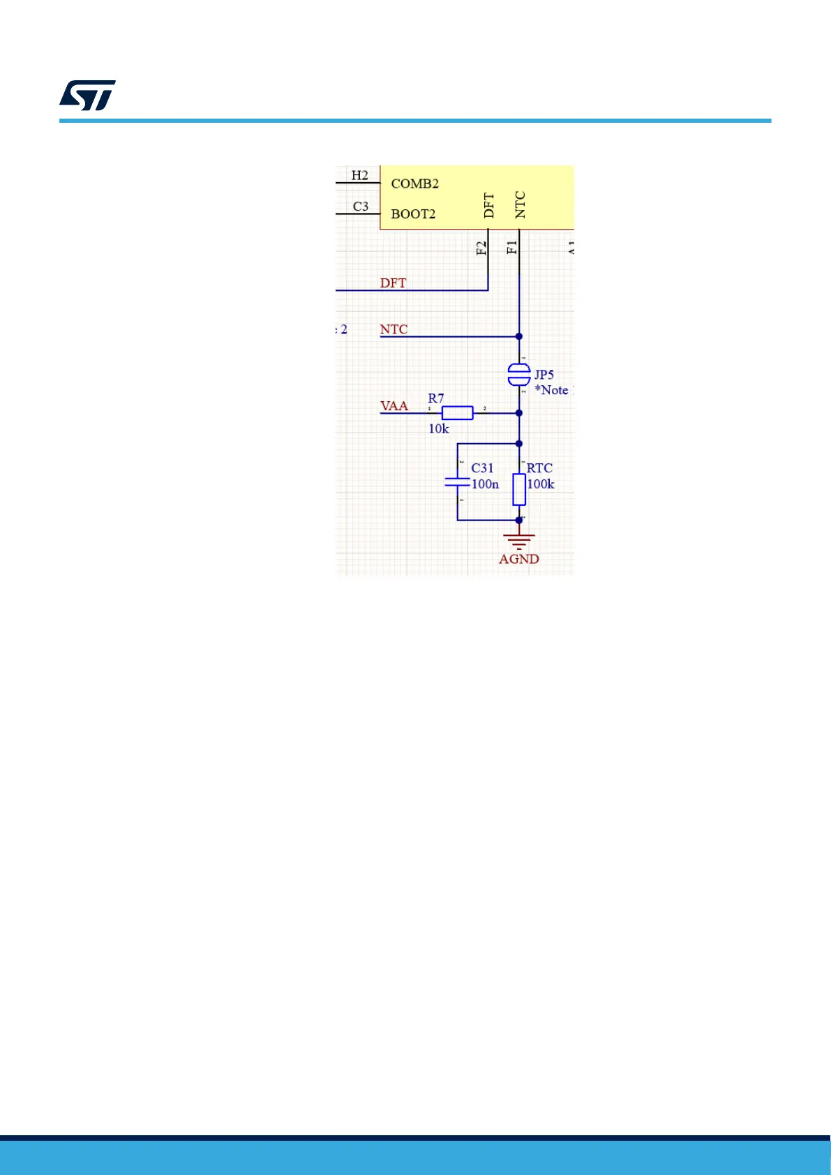
Figure 64. External NTC connection
9.2 PCB layout guidelines
• Power tracks (AC1, AC2, VRECT, VOUT) and power ground tracks should be kept wide enough to sustain
high current. Duplicating these tracks in inner layers and adding vias is advisable wherever possible to
lower impedance as much as possible.
• AC1, AC2, BOOT1, BOOT2, COMAx, and COMBx generate noise. Using shielding near these traces (by
placing ground planes below) is recommended.
• Power ground carries the sum of ripple current from VRECT/Crect and DC current from VOUT/Load.
Current return paths from LDO capacitors should be routed separately from the high current paths.
• AC1 and AC2 tracks should be routed close together to minimize the area of the resulting loop.
• Communication (I
2
C) and sensing signals should be routed far from noise generating nets (AC1, AC2,
COMAx, COMBx, BOOT) to minimize the effects of interference induced from those high di/dt nets.
• COMM1, COMM2, BOOT1, BOOT2 capacitors should be placed as close to the device as possible.
• VRECT and VOUT capacitors should be placed close to the device to minimize the area of high current
loops.
• Auxiliary LDO capacitors should be placed as close to the device as possible.
• Thermal performance and grounding can be enhanced by dedicating one layer as a ground plane. No
signal/power tracks should be routed on this layer to ensure ground integrity.
9.3
LDO output voltage configuration
Configuration of the LDO has a major impact on efficiency, as it directly affects the magnitude of the power loss
created by the passing current. Therefore, minimizing the voltage drop is desired when aiming for higher
efficiency.
However, a higher LDO drop improves communication stability and helps prevent negative modulation, which
might leak into the output voltage. Lastly, different rectifier operating modes also affect the VRECT waveform.
Therefore, LDO drop configuration is a tradeoff between efficiency and communication/output voltage stability.
UM3154
PCB layout guidelines
UM3154 - Rev 2
page 58/81