DocID026079 Rev 3 53/102
STM32F038x6 Electrical characteristics
79
Figure 13. High-speed external clock source AC timing diagram
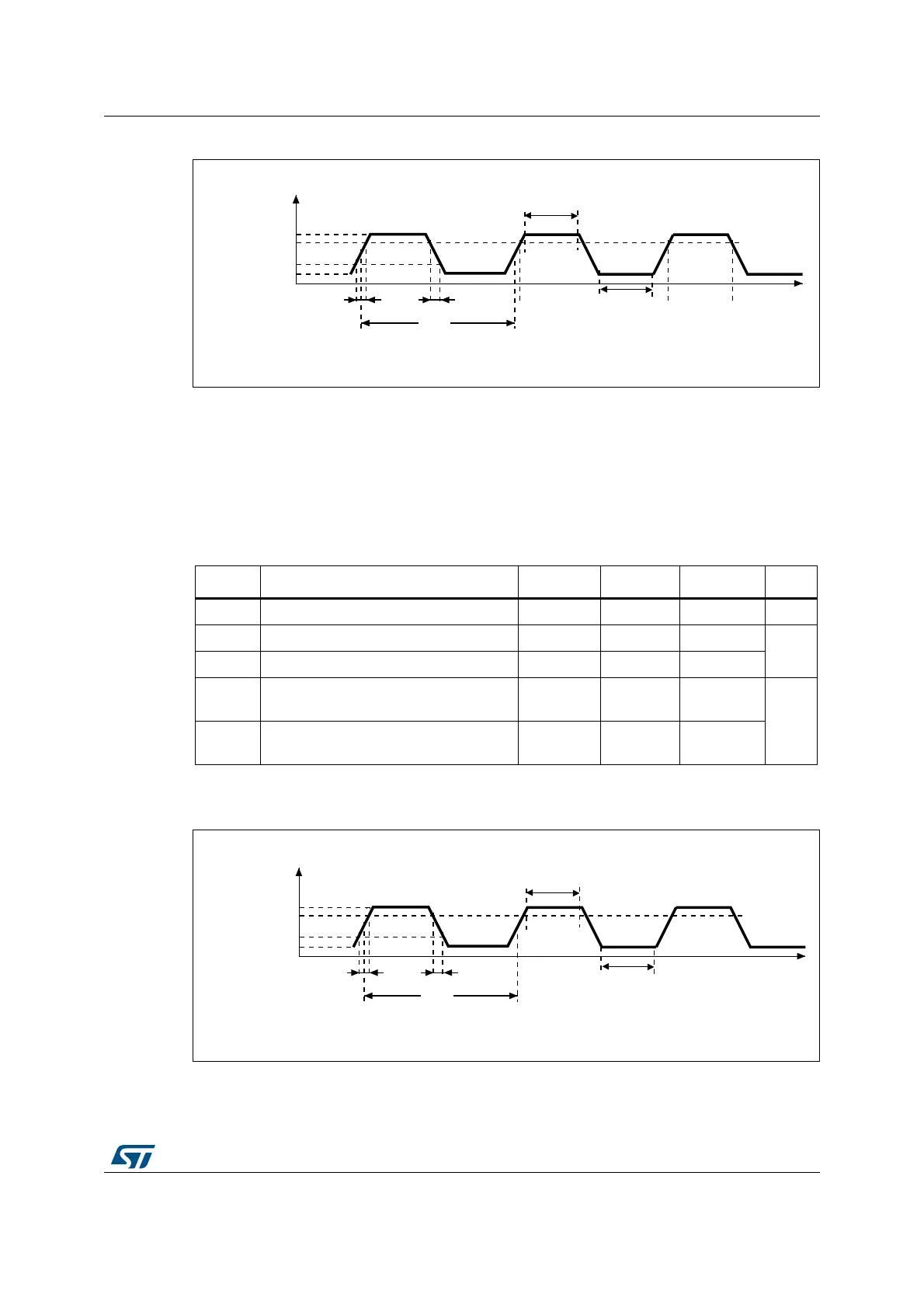
Low-speed external user clock generated from an external source
In bypass mode the LSE oscillator is switched off and the input pin is a standard GPIO.
The external clock signal has to respect the I/O characteristics in Section 6.3.13. However,
the recommended clock input waveform is shown in Figure 14.
Figure 14. Low-speed external clock source AC timing diagram
Table 30. Low-speed external user clock characteristics
Symbol Parameter
(1)
1. Guaranteed by design, not tested in production.
Min Typ Max Unit
f
LSE_ext
User external clock source frequency - 32.768 1000 kHz
V
LSEH
OSC32_IN input pin high level voltage 0.7 V
DDIOx
-V
DDIOx
V
V
LSEL
OSC32_IN input pin low level voltage V
SS
- 0.3 V
DDIOx
t
w(LSEH)
t
w(LSEL)
OSC32_IN high or low time 450 - -
ns
t
r(LSE)
t
f(LSE)
OSC32_IN rise or fall time - - 50
069
9
+6(+
W
I+6(
7
+6(
W
W
U+6(
9
+6(/
W
Z+6(+
W
Z+6(/
069
9
/6(+
W
I/6(
7
/6(
W
W
U/6(
9
/6(/
W
Z/6(+
W
Z/6(/