Package information STM32F038x6
90/102 DocID026079 Rev 3
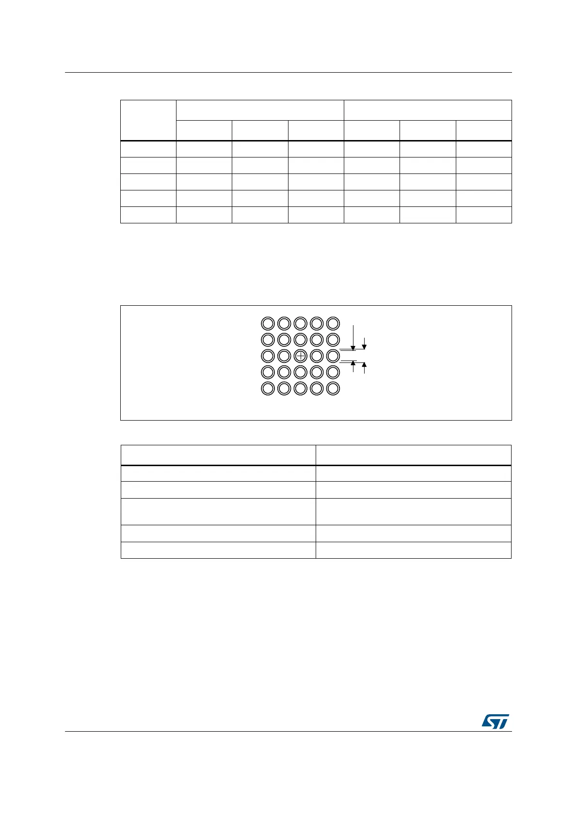
Figure 40. Recommended footprint for WLCSP25 package
aaa - 0.100 - - 0.0039 -
bbb - 0.100 - - 0.0039 -
ccc - 0.100 - - 0.0039 -
ddd - 0.050 - - 0.0020 -
eee - 0.050 - - 0.0020 -
1. Values in inches are converted from mm and rounded to 4 decimal digits.
2. Back side coating.
3. Dimension is measured at the maximum bump diameter parallel to primary datum Z.
4. Primary datum Z and seating plane are defined by the spherical crowns of the bump.
Table 64. WLCSP25 recommended PCB design rules
Dimension Recommended values
Pitch 0.4 mm
Dpad 0.225 mm
Dsm
0.290 mm typ. (depends on the soldermask
registration tolerance)
Stencil opening 0.250 mm
Stencil thickness 0.100 mm
Table 63. WLCSP25 package mechanical data (continued)
Symbol
millimeters inches
(1)
Min Typ Max Min Typ Max
:/&63B$1B)3B9
'SDG
'VP