DocID026079 Rev 3 63/102
STM32F038x6 Electrical characteristics
79
6.3.13 I/O port characteristics
General input/output characteristics
Unless otherwise specified, the parameters given in Table 44 are derived from tests
performed under the conditions summarized in Table 18: General operating conditions. All
I/Os are designed as CMOS- and TTL-compliant (except BOOT0).
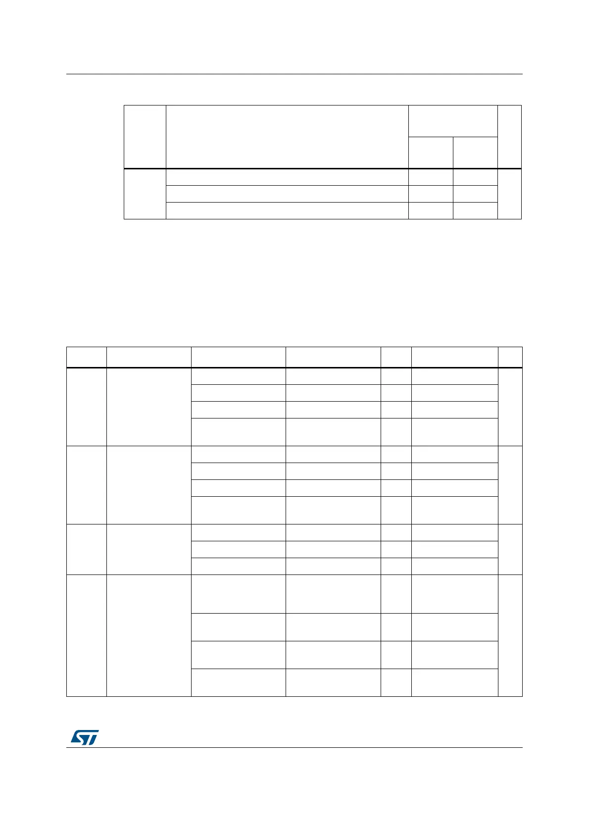
Table 43. I/O current injection susceptibility
Symbol Description
Functional
susceptibility
Unit
Negative
injection
Positive
injection
I
INJ
Injected current on BOOT0 –0 NA
mAInjected current on all FT, FTf and POR pins –5 NA
Injected current on all TTa, TC and RESET pins –5 +5
Table 44. I/O static characteristics
Symbol Parameter Conditions Min Typ Max Unit
V
IL
Low level input
voltage
TC and TTa I/O - - 0.3 V
DDIOx
+0.07
(1)
V
FT and FTf I/O - - 0.475 V
DDIOx
–0.2
(1)
BOOT0 - - 0.3 V
DDIOx
–0.3
(1)
All I/Os except
BOOT0 pin
--0.3 V
DDIOx
V
IH
High level input
voltage
TC and TTa I/O 0.445 V
DDIOx
+0.398
(1)
--
V
FT and FTf I/O 0.5 V
DDIOx
+0.2
(1)
--
BOOT0 0.2 V
DDIOx
+0.95
(1)
--
All I/Os except
BOOT0 pin
0.7 V
DDIOx
--
V
hys
Schmitt trigger
hysteresis
TC and TTa I/O - 200
(1)
-
mVFT and FTf I/O - 100
(1)
-
BOOT0 - 300
(1)
-
I
lkg
Input leakage
current
(2)
TC, FT and FTf I/O
TTa in digital mode
V
SS
≤ V
IN
≤ V
DDIOx
--± 0.1
µA
TTa in digital mode
V
DDIOx
≤ V
IN
≤ V
DDA
--1
TTa in analog mode
V
SS
≤ V
IN
≤ V
DDA
--± 0.2
FT and FTf I/O
V
DDIOx
≤ V
IN
≤ 5 V
--10