Electrical characteristics STM32F038x6
42/102 DocID026079 Rev 3
6.3.2 Operating conditions at power-up / power-down
The parameters given in Table 19 are derived from tests performed under the ambient
temperature condition summarized in Table 18.
6.3.3 Embedded reference voltage
The parameters given in Table 20 are derived from tests performed under the ambient
temperature and supply voltage conditions summarized in Table 18: General operating
conditions.
6.3.4 Supply current characteristics
The current consumption is a function of several parameters and factors such as the
operating voltage, ambient temperature, I/O pin loading, device software configuration,
operating frequencies, I/O pin switching rate, program location in memory and executed
binary code.
The current consumption is measured as described in Figure 12: Current consumption
measurement scheme.
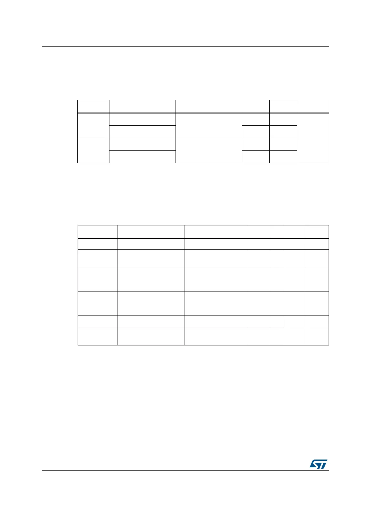
Table 19. Operating conditions at power-up / power-down
Symbol Parameter Conditions Min Max Unit
t
VDD
V
DD
rise time rate
-
0
∞
µs/V
V
DD
fall time rate 20
∞
t
VDDA
V
DDA
rise time rate
-
0
∞
V
DDA
fall time rate 20
∞
Table 20. Embedded internal reference voltage
Symbol Parameter Conditions Min Typ Max Unit
V
REFINT
Internal reference voltage –40 °C < T
A
< +105 °C 1.16 1.2 1.25 V
t
START
ADC_IN17 buffer startup
time
---10
(1)
µs
t
S_vrefint
ADC sampling time when
reading the internal
reference voltage
-
4
(1)
1. Guaranteed by design, not tested in production.
-- µs
ΔV
REFINT
Internal reference voltage
spread over the
temperature range
V
DDA
= 3 V - -
10
(1)
mV
T
Coeff
Temperature coefficient -
- 100
(1)
-
100
(1)
ppm/°C
T
VREFINT_RDY
(2)
2. Guaranteed by design, not tested in production. This parameter is the latency between the time when pin
NPOR is set to 1 by the application and the time when the VREFINTRDYF status bit is set to 1 by the
hardware.
Internal reference voltage
temporization
- 1.5 2.5 4.5 ms