DocID026079 Rev 3 75/102
STM32F038x6 Electrical characteristics
79
SPI/I
2
S characteristics
Unless otherwise specified, the parameters given in Table 58 for SPI or in Table 59 for I
2
S
are derived from tests performed under the ambient temperature, f
PCLKx
frequency and
supply voltage conditions summarized in
Table 18: General operating conditions.
Refer to Section 6.3.13: I/O port characteristics for more details on the input/output alternate
function characteristics (NSS, SCK, MOSI, MISO for SPI and WS, CK, SD for I
2
S).
Table 57. I
2
C analog filter characteristics
(1)
1. Guaranteed by design, not tested in production.
Symbol Parameter Min Max Unit
t
AF
Maximum width of spikes that are
suppressed by the analog filter
50
(2)
2. Spikes with widths below t
AF(min)
are filtered.
260
(3)
3. Spikes with widths above t
AF(max)
are not filtered
ns
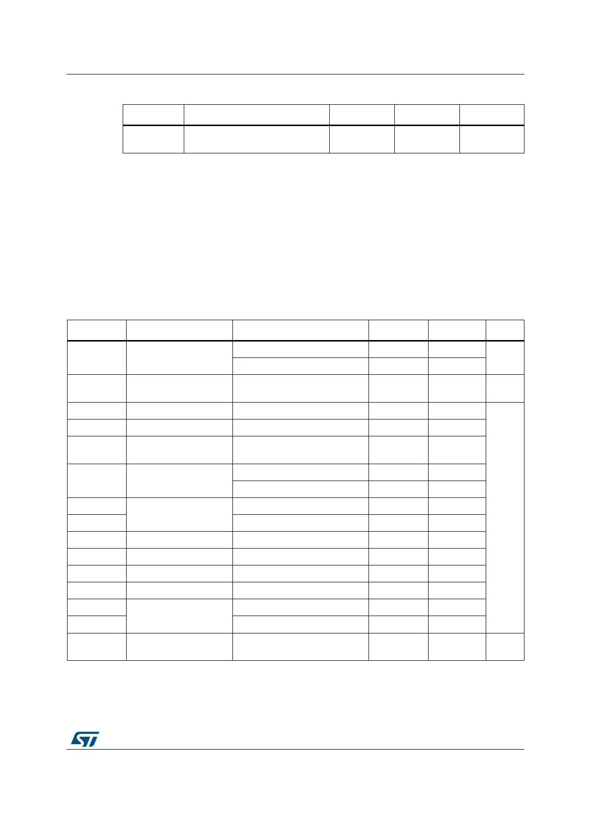
Table 58. SPI characteristics
(1)
Symbol Parameter Conditions Min Max Unit
f
SCK
1/t
c(SCK)
SPI clock frequency
Master mode - 18
MHz
Slave mode - 18
t
r(SCK)
t
f(SCK)
SPI clock rise and fall
time
Capacitive load: C = 15 pF - 6 ns
t
su(NSS)
NSS setup time Slave mode 4Tpclk -
ns
t
h(NSS)
NSS hold time Slave mode 2Tpclk + 10 -
t
w(SCKH)
t
w(SCKL)
SCK high and low time
Master mode, f
PCLK
= 36 MHz,
presc = 4
Tpclk/2 -2 Tpclk/2 + 1
t
su(MI)
t
su(SI)
Data input setup time
Master mode 4 -
Slave mode 5 -
t
h(MI)
Data input hold time
Master mode 4 -
t
h(SI)
Slave mode 5 -
t
a(SO)
(2)
Data output access time Slave mode, f
PCLK
= 20 MHz 0 3Tpclk
t
dis(SO)
(3)
Data output disable time Slave mode 0 18
t
v(SO)
Data output valid time Slave mode (after enable edge) - 22.5
t
v(MO)
Data output valid time Master mode (after enable edge) - 6
t
h(SO)
Data output hold time
Slave mode (after enable edge) 11.5 -
t
h(MO)
Master mode (after enable edge) 2 -
DuCy(SCK)
SPI slave input clock
duty cycle
Slave mode 25 75 %
1. Data based on characterization results, not tested in production.
2. Min time is for the minimum time to drive the output and the max time is for the maximum time to validate the data.
3. Min time is for the minimum time to invalidate the output and the max time is for the maximum time to put the data in Hi-Z