Electrical characteristics STM32F038x6
52/102 DocID026079 Rev 3
6.3.5 Wakeup time from low-power mode
The wakeup times given in Table 28 are the latency between the event and the execution of
the first user instruction. The device goes in low-power mode after the WFE (Wait For
Event) instruction, in the case of a WFI (Wait For Interruption) instruction, 16 CPU cycles
must be added to the following timings due to the interrupt latency in the Cortex M0
architecture.
The SYSCLK clock source setting is kept unchanged after wakeup from Sleep mode.
During wakeup from Stop mode, SYSCLK takes the default setting: HSI 8 MHz.
The wakeup source from Sleep and Stop mode is an EXTI line configured in event mode.
All timings are derived from tests performed under the ambient temperature and supply
voltage conditions summarized in
Table 18: General operating conditions..
6.3.6 External clock source characteristics
High-speed external user clock generated from an external source
In bypass mode the HSE oscillator is switched off and the input pin is a standard GPIO.
The external clock signal has to respect the I/O characteristics in Section 6.3.13. However,
the recommended clock input waveform is shown in Figure 13: High-speed external clock
source AC timing diagram.
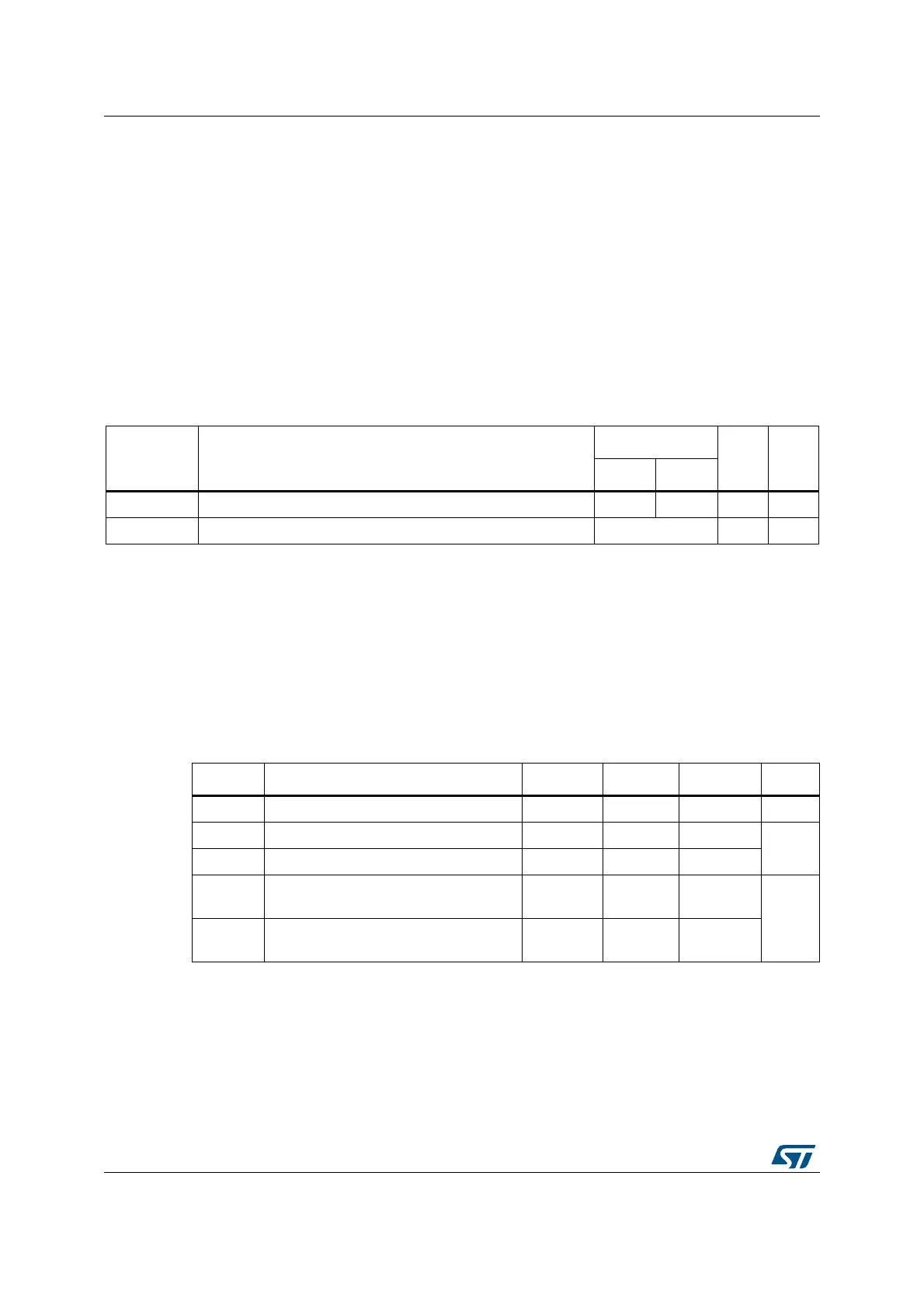
Table 28. Low-power mode wakeup timings
Symbol Parameter
Typ @ V
DDA
Max Unit
= 1.8 V = 3.3 V
t
WUSTOP
Wakeup from Stop mode 3.5 2.8 5.3 µs
t
WUSLEEP
Wakeup from Sleep mode 4 SYSCLK cycles - µs
Table 29. High-speed external user clock characteristics
Symbol Parameter
(1)
1. Guaranteed by design, not tested in production.
Min Typ Max Unit
f
HSE_ext
User external clock source frequency - 8 32 MHz
V
HSEH
OSC_IN input pin high level voltage 0.7 V
DDIOx
-V
DDIOx
V
V
HSEL
OSC_IN input pin low level voltage V
SS
- 0.3 V
DDIOx
t
w(HSEH)
t
w(HSEL)
OSC_IN high or low time 15 - -
ns
t
r(HSE)
t
f(HSE)
OSC_IN rise or fall time - - 20