DocID026079 Rev 3 73/102
STM32F038x6 Electrical characteristics
79
6.3.16 Temperature sensor characteristics
6.3.17 V
BAT
monitoring characteristics
6.3.18 Timer characteristics
The parameters given in the following tables are guaranteed by design.
Refer to Section 6.3.13: I/O port characteristics for details on the input/output alternate
function characteristics (output compare, input capture, external clock, PWM output).
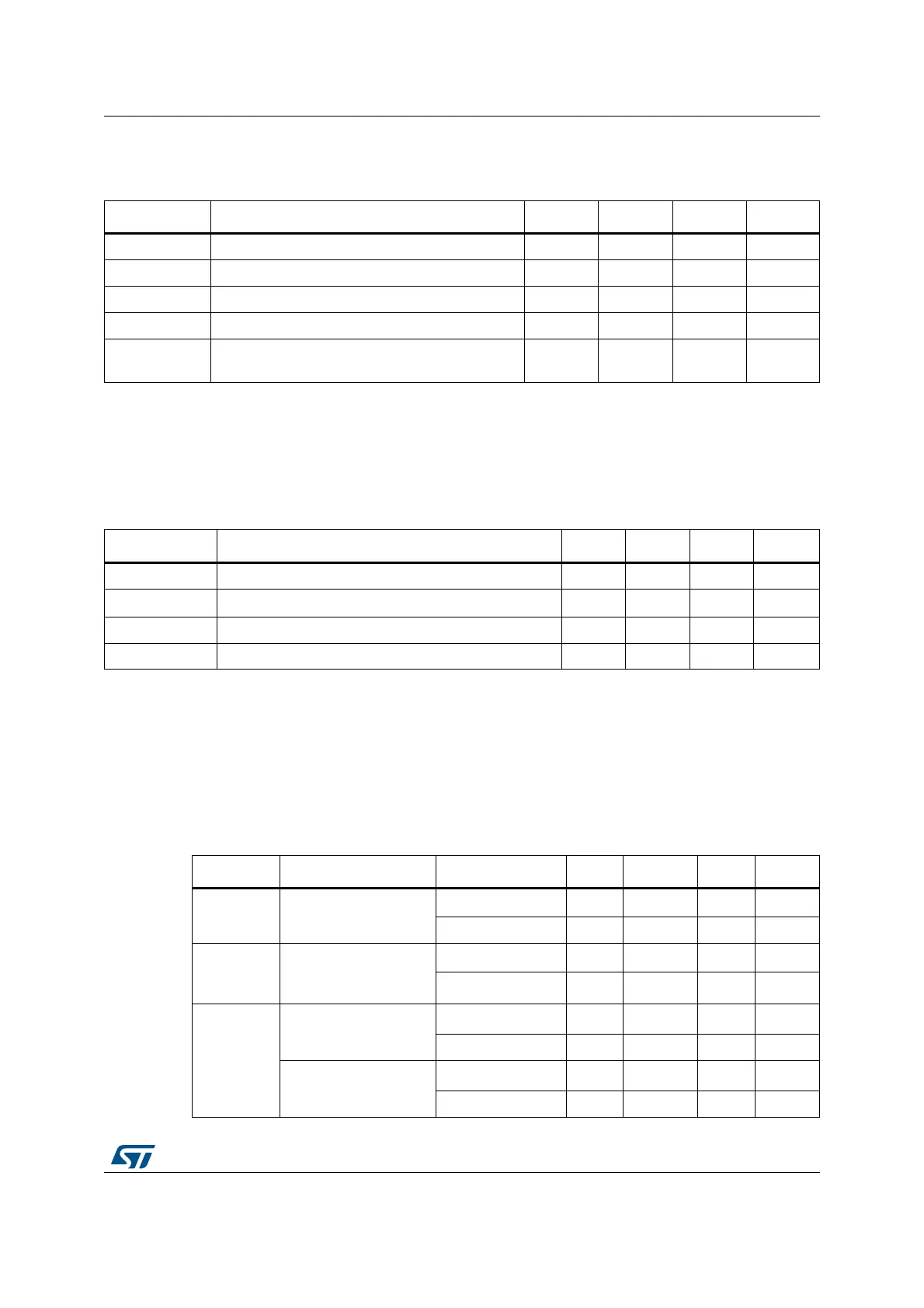
Table 52. TS characteristics
Symbol Parameter Min Typ Max Unit
T
L
(1)
V
SENSE
linearity with temperature - ± 1 ± 2°C
Avg_Slope
(1)
Average slope 4.0 4.3 4.6 mV/°C
V
30
Voltage at 30 °C (± 5 °C)
(2)
1.34 1.43 1.52 V
t
START
(1)
ADC_IN16 buffer startup time - - 10 µs
t
S_temp
(1)
ADC sampling time when reading the
temperature
4--µs
1. Guaranteed by design, not tested in production.
2. Measured at V
DDA
= 3.3 V ± 10 mV. The V
30
ADC conversion result is stored in the TS_CAL1 byte. Refer to Table 3:
Temperature sensor calibration values.
Table 53. V
BAT
monitoring characteristics
Symbol Parameter Min Typ Max Unit
R Resistor bridge for V
BAT
-2 x 50- kΩ
Q
Ratio on V
BAT
measurement - 2 -
Er
(1)
Error on Q –1 - +1 %
t
S_vbat
(1)
ADC sampling time when reading the V
BAT
4--µs
1. Guaranteed by design, not tested in production.
Table 54. TIMx characteristics
Symbol Parameter Conditions Min Typ Max Unit
t
res(TIM)
Timer resolution time
--1-
t
TIMxCLK
f
TIMxCLK
= 48 MHz - 20.8 - ns
f
EXT
Timer external clock
frequency on CH1 to
CH4
--
f
TIMxCLK
/2
-MHz
f
TIMxCLK
= 48 MHz - 24 - MHz
t
MAX_COUNT
16-bit timer maximum
period
--
2
16
-
t
TIMxCLK
f
TIMxCLK
= 48 MHz - 1365 - µs
32-bit counter
maximum period
--
2
32
-
t
TIMxCLK
f
TIMxCLK
= 48 MHz - 89.48 - s