Electrical characteristics STM32F038x6
78/102 DocID026079 Rev 3
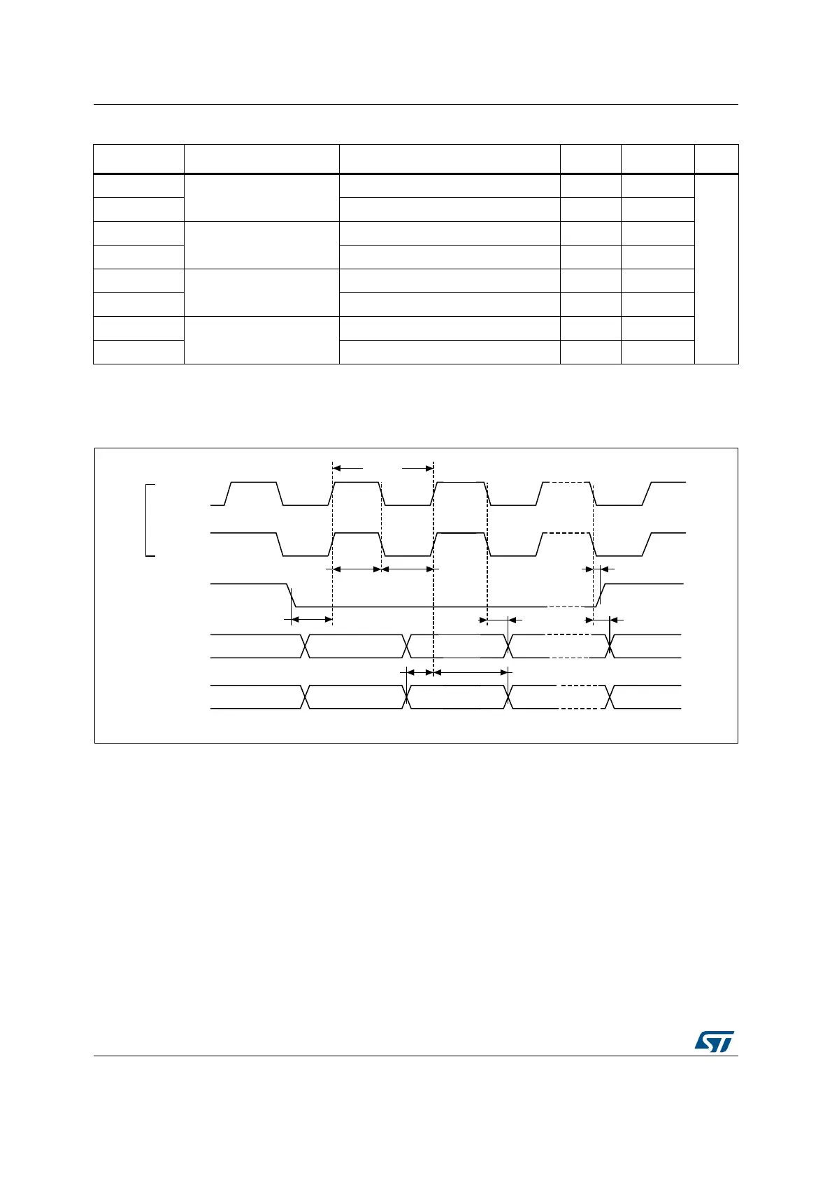
Figure 28. I
2
S slave timing diagram (Philips protocol)
1. Measurement points are done at CMOS levels: 0.3 × V
DDIOx
and 0.7 × V
DDIOx
.
2. LSB transmit/receive of the previously transmitted byte. No LSB transmit/receive is sent before the first
byte.
t
su(SD_MR)
Data input setup time
Master receiver 6 -
ns
t
su(SD_SR)
Slave receiver 2 -
t
h(SD_MR)
(2)
Data input hold time
Master receiver 4 -
t
h(SD_SR)
(2)
Slave receiver 0.5 -
t
v(SD_MT)
(2)
Data output valid time
Master transmitter - 4
t
v(SD_ST)
(2)
Slave transmitter - 31
t
h(SD_MT)
Data output hold time
Master transmitter 0 -
t
h(SD_ST)
Slave transmitter 13 -
1. Data based on design simulation and/or characterization results, not tested in production.
2. Depends on f
PCLK
. For example, if f
PCLK
= 8 MHz, then T
PCLK
= 1/f
PLCLK
= 125 ns.
Table 59. I
2
S characteristics
(1)
(continued)
Symbol Parameter Conditions Min Max Unit
06Y9
&.,QSXW
&32/
&32/
WF&.
:6LQSXW
6'WUDQVPLW
6'UHFHLYH
WZ&.+
WZ&./
WVX:6
WY6'B67 WK6'B67
WK:6
WVX6'B65 WK6'B65
06%UHFHLYH %LWQUHFHLYH /6%UHFHLYH
06%WUDQVPLW %LWQWUDQVPLW
/6%UHFHLYH
/6%WUDQVPLW