DocID026079 Rev 3 69/102
STM32F038x6 Electrical characteristics
79
6.3.15 12-bit ADC characteristics
Unless otherwise specified, the parameters given in Table 49 are derived from tests
performed under the conditions summarized in Table 18: General operating conditions.
Note: It is recommended to perform a calibration after each power-up.
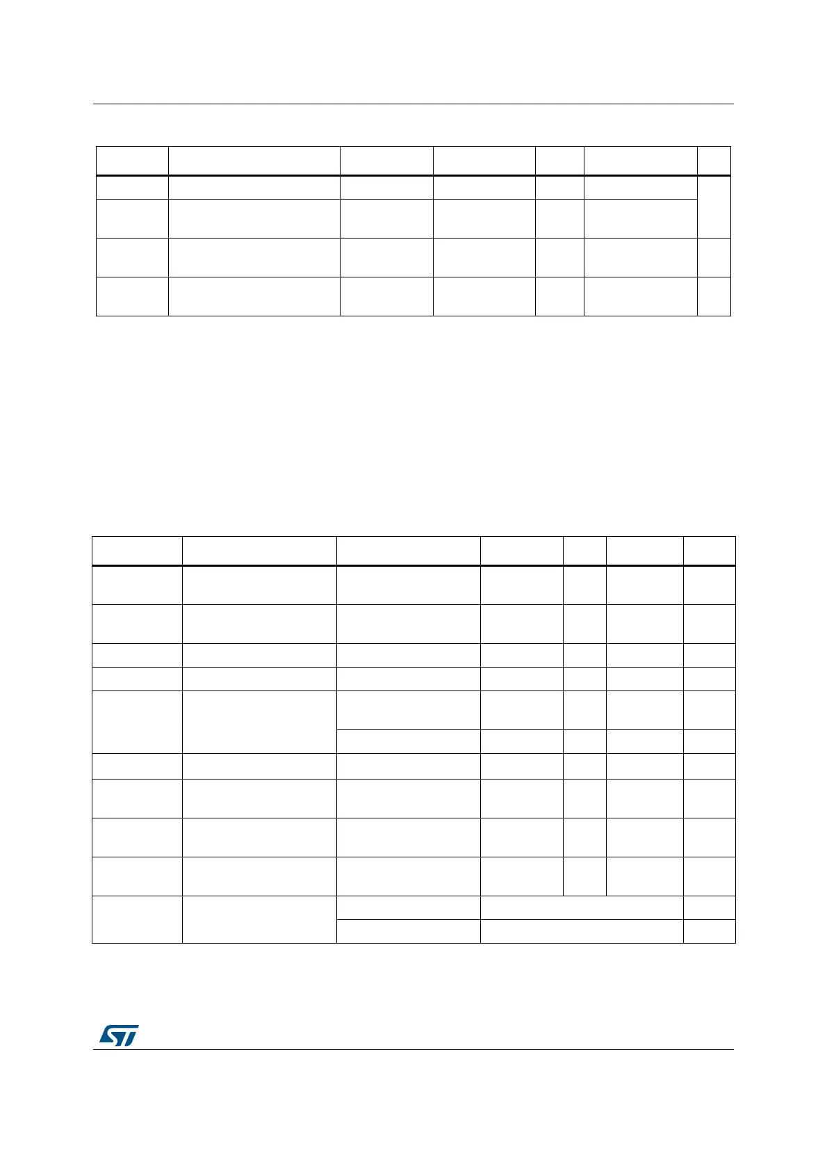
Table 48. NPOR pin characteristics
Symbol Parameter Conditions Min Typ Max Unit
V
IL(NPOR)
NPOR Input low level voltage - 0.475 V
DDA
- 0.2
(1)
V
V
IH(NPOR)
NPOR Input high level
voltage
0.5 V
DDA
+ 0.2
(1)
-
V
hys(NPOR)
NPOR Schmitt trigger voltage
hysteresis
--100
(1)
-mV
R
PU
Weak pull-up equivalent
resistor
(2)
V
IN
= V
SS
25 40 55 kΩ
1. Guaranteed by design, not tested in production.
2. The pull-up is designed with a true resistance in series with a switchable PMOS. This PMOS contribution to the series
resistance is minimal (~10% order).
Table 49. ADC characteristics
Symbol Parameter Conditions Min Typ
Max Unit
V
DDA
Analog supply voltage for
ADC ON
- 2.4 - 3.6 V
I
DDA (ADC)
Current consumption of
the ADC
(1)
V
DDA
= 3.3 V - 0.9 - mA
f
ADC
ADC clock frequency - 0.6 - 14 MHz
f
S
(2)
Sampling rate 12-bit resolution 0.043 - 1 MHz
f
TRIG
(2)
External trigger frequency
f
ADC
= 14 MHz,
12-bit resolution
--823kHz
12-bit resolution - - 17 1/f
ADC
V
AIN
Conversion voltage range - 0 - V
DDA
V
R
AIN
(2)
External input impedance
See Equation 1 and
Table 50 for details
--50kΩ
R
ADC
(2)
Sampling switch
resistance
---1kΩ
C
ADC
(2)
Internal sample and hold
capacitor
---8pF
t
CAL
(2)(3)
Calibration time
f
ADC
= 14 MHz 5.9 µs
-831/f
ADC