DocID026079 Rev 3 71/102
STM32F038x6 Electrical characteristics
79
28.52.0425.2
41.52.9637.2
55.5 3.96 50
71.5 5.11 NA
239.5 17.1 NA
1. Guaranteed by design, not tested in production.
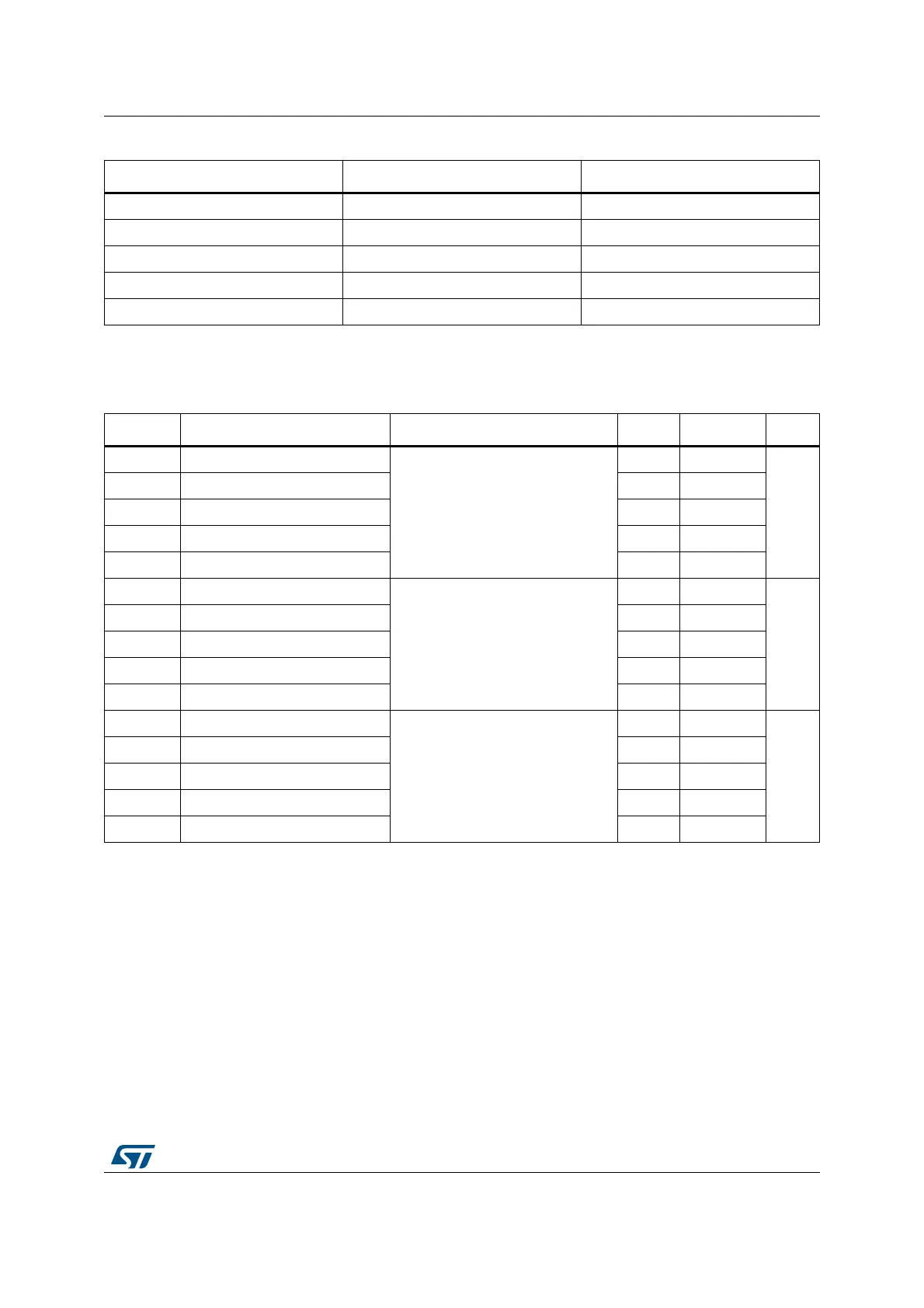
Table 50. R
AIN
max for f
ADC
= 14 MHz (continued)
T
s
(cycles) t
S
(µs) R
AIN
max (kΩ)
(1)
Table 51. ADC accuracy
(1)(2)(3)
Symbol Parameter Test conditions Typ Max
(4)
Unit
ET Total unadjusted error
f
PCLK
= 48 MHz,
f
ADC
= 14 MHz, R
AIN
< 10 kΩ
V
DDA
= 3 V to 3.6 V
T
A
= 25 °C
±1.3 ±2
LSB
EO Offset error ±1 ±1.5
EG Gain error ±0.5 ±1.5
ED Differential linearity error ±0.7 ±1
EL Integral linearity error ±0.8 ±1.5
ET Total unadjusted error
f
PCLK
= 48 MHz,
f
ADC
= 14 MHz, R
AIN
< 10 kΩ
V
DDA
= 2.7 V to 3.6 V
T
A
= −40 to 105 °C
±3.3 ±4
LSB
EO Offset error ±1.9 ±2.8
EG Gain error ±2.8 ±3
ED Differential linearity error ±0.7 ±1.3
EL Integral linearity error ±1.2 ±1.7
ET Total unadjusted error
f
PCLK
= 48 MHz,
f
ADC
= 14 MHz, R
AIN
< 10 kΩ
V
DDA
= 2.4 V to 3.6 V
T
A
= 25 °C
±3.3 ±4
LSB
EO Offset error ±1.9 ±2.8
EG Gain error ±2.8 ±3
ED Differential linearity error ±0.7 ±1.3
EL Integral linearity error ±1.2 ±1.7
1. ADC DC accuracy values are measured after internal calibration.
2. ADC Accuracy vs. Negative Injection Current: Injecting negative current on any of the standard (non-robust) analog input
pins should be avoided as this significantly reduces the accuracy of the conversion being performed on another analog
input. It is recommended to add a Schottky diode (pin to ground) to standard analog pins which may potentially inject
negative current.
Any positive injection current within the limits specified for I
INJ(PIN)
and ΣI
INJ(PIN)
in Section 6.3.13 does not affect the ADC
accuracy.
3. Better performance may be achieved in restricted V
DDA
, frequency and temperature ranges.
4. Data based on characterization results, not tested in production.