p
Model 880 DEPOSITION CONTROLLER
y
SECTION 4.XX
e page 145 of 275 ^
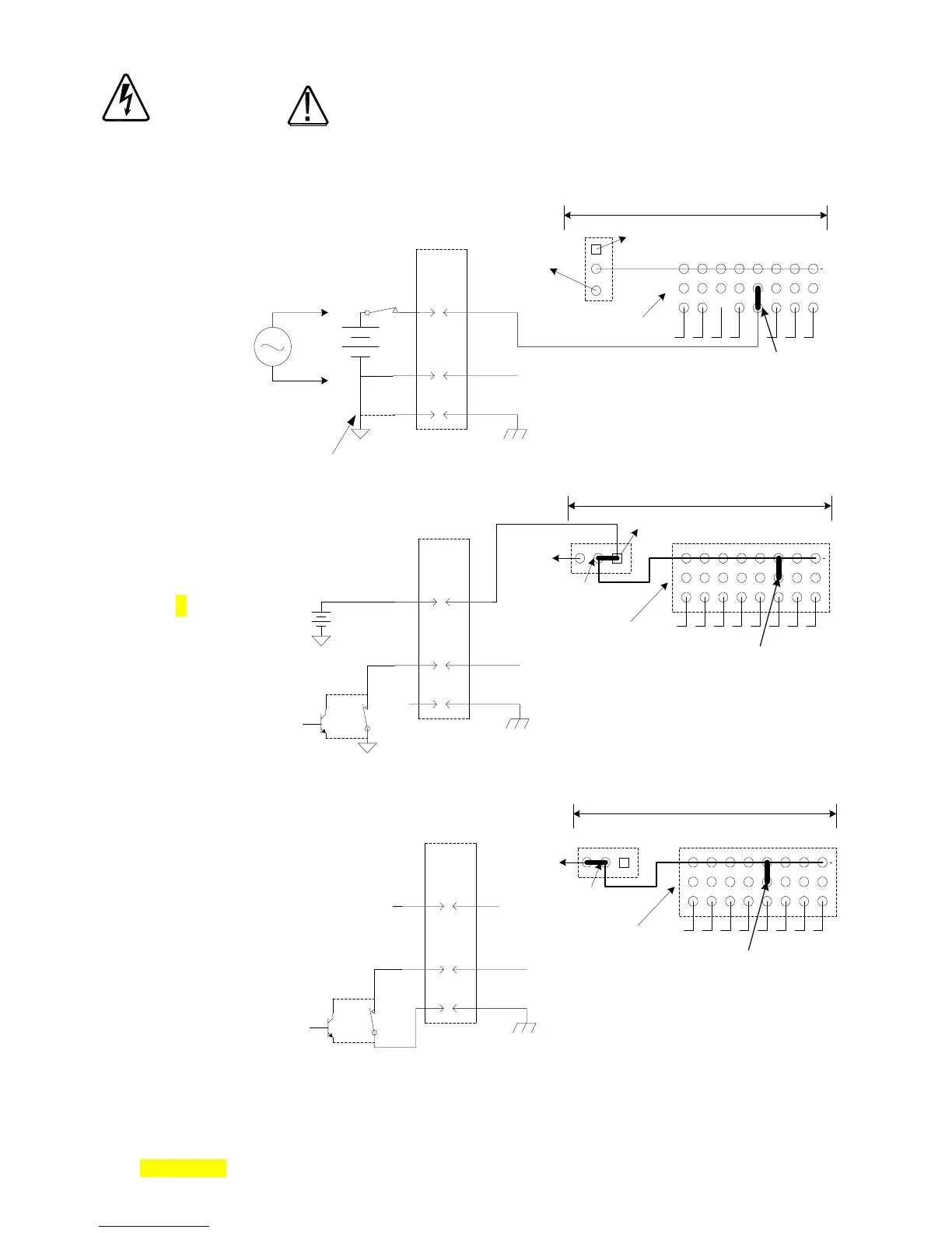
JP2
JP1
5VDC ext
5VDC
1A
1B
1C
8A
8B
8C
(Internal Vcc)
(row C is closest to PC board)
+ Inputs to Opto Circuits
are on Row B
pin 19
pin 6
-
Input 4
+
Input 4
Two Pin Shorting
Block Located
Here for
+
Input 4
DG
2002 TFC ground
Optocoupler
Inputs DB25F
Connector
3.5V<VDC<40V
Isolated
external
ground
pin 13
Optional:
Connect grounds for
non-isolated hookup
Optional AC Input:
5<Vrms<30
50 - 60 Hz
CONNECTIONS FOR AC OR DC
USING INPUT 4
JP2
JP1
5VDC ext
5VDC
1A
1B
1C
8A
8B
8C
(Internal Vcc)
(row C is closest to PC board)
+ Inputs to Opto Circuits
are on Row B
pin 1
pin 17
-
Input 3
Two Pin Shorting
Block Located Here
for
+
Input 3
Connection to +5VDC
DG
2002 TFC ground
Optocoupler
Inputs DB25F
Connector
Isolated
external
ground
pin 13
CONNECTIONS FOR CLOSURE TO
ISOLATED GROUND FOR INPUT 3
Shorting
Block
+5VDC
EXT.
NC
Open
Collector
Contact
JP2
JP1
5VDC ext
5VDC
1A
1B
1C
8A
8B
8C
(Internal Vcc)
(row C is closest to PC board)
+ Inputs to Opto Circuits
are on Row B
pin 1
pin 6
-
Input 4
Two Pin Shorting
Block Located Here
for
+
Input 4
Connection to +5VDC
DG
2002 TFC ground
Optocoupler
Inputs DB25F
Connector
pin 13
CONNECTIONS FOR CLOSURE TO
NON-ISOLATED GROUND FOR INPUT 4
Shorting
Block
NC
Open
Collector
Contact
(or Logic Level)
2002 TFC Input Module PC-Board
2002 TFC Input Module PC-Board
2002 TFC Input Module PC-Board
Input PCB
Card jumper
installation:
See section 7
for shock
hazard and
ESD
sensitivity
Static
Sensitive
Hazardous
Voltages
Present
Figure- 4.6: Examples of Shorting Block Locations to Accommodate the Various
Optocoupler Input Hookup Options