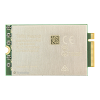
FN990
Family Hardware Design Guide
1VV0301752 Rev. 3 Page 47 of 92 2022-10-07
Not Sub
ect to NDA
Warning: FN990 data cards are not designed or intended to support
Hot-Swap or Hot-Plug connection. Performing How-Swap or Hot-
Plug may pose danger to the FN990 Family module, to the host
device, and to the person handling the device.
6.3.1.2.1. PCIe Layout Guidelines
This guidelines will provide general guidelines for PCIe interface to improve signal
integrity.
All other sensitive/high-speed signals and cicuits must be protected from PCIe
corruption
PCIe signals must be protected from noisy signals (clocks, SMPS, and so forth)
Pay extra attention to crosstalk, ISI, and intralane skew and impedance
discontinuities.
PCIe Tx AC copling capacitors are better placed close to the source or receiver
side to keep good SI of route on PCB.
To maintain impedance balance, maintain positive and negative traces as
balanced as possible in terms of the signal and its return path.
Trace length matching between the reference clock, Tx, and Rx pairs are not
required.
External capacitors also should keep differential traces. Ensure not to stagger
the capacitors. This can affect the differential integrity of the design and can
create EMI.
Type of guidance Guideline Requirement
General Data rate 8 Gbps*
Insertion loss at 4 GHz (dB) -10 dB
Impedance 85 ohms differential
Bus length 285 mm**
Length matching Intra pair match < 0.7mm
Spacing To all other signals > 4 x line width
Tx lane to Rx lane > 4 x line width
Component AC capacitance 220 nF
Table 31: PCIe Routing Constraints
*Actual throughput at the system level could be lower due to overheads.
**PCIe trace length in FN990 Family: about 15 mm.

 Loading...