4.11.2 X2 Lane PCIe Interface
The x2 lane PCIe interface includes one x4 lane PCIe connector of part number Amphenol 10142333-10111MLF,
which supports PCIe Gen4 operation. The pin-out of the connector follows PCIe standard.
The SERDES1 port of J7 SoC is connected to x1 lane PCIe socket for data transfer. PCIe1, USB1_SS,
PRG1_SGMII0, 1 and SGMII3, 4 interfaces are pinmuxed with this SERDES1 port.
Figure 4-23. PCIe Interface for SERDES1
I2C0 from SoC is used for control purposes and is connected to SMBUS on the connector through I2C switch.
The link activation signal (INT#) from both the X1 and X2 lane PCIe connectors is terminated to I2C switch.
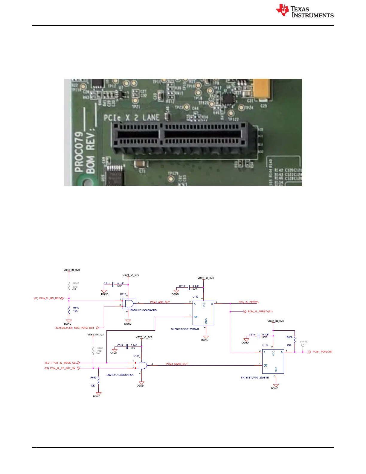
Reset: A dip Switch (SW3) is provided to select the reset source for host and end-point PCIe operation.
In case of host mode, signal from GPIO Expander and PORz signals from SoC are ANDed and the output is
connected to PCIe connector. The GPIO signal is pulled low to ensure PCIe Reset (#PERST) remains asserted
until SoC releases reset.
Whereas, in case of PCIe end point operation, the CP board receives reset signal from the PCIe card.
Figure 4-24. 2L-PCIe Root Complex/Endpoint Selection Circuit
J721E EVM Hardware Architecture www.ti.com
56 Jacinto7 J721E/DRA829/TDA4VM Evaluation Module (EVM) SPRUIS4D – MAY 2020 – REVISED MARCH 2022
Submit Document Feedback
Copyright © 2022 Texas Instruments Incorporated