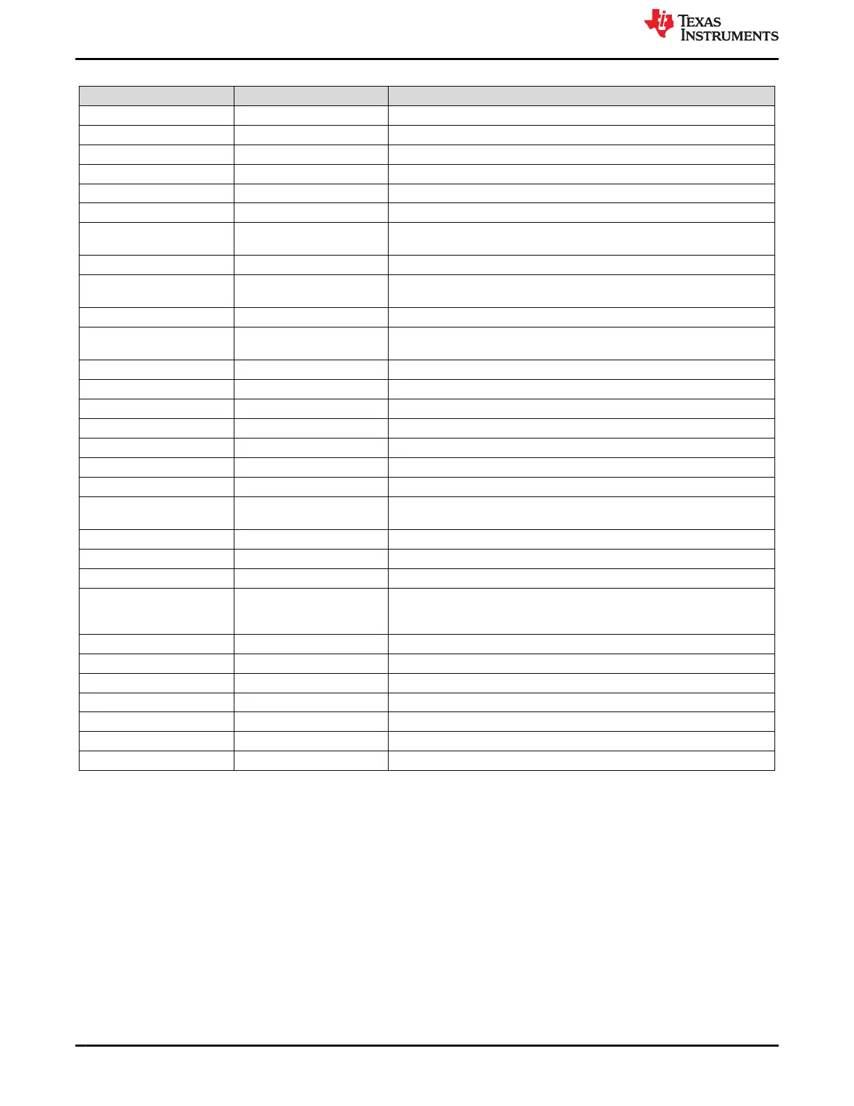
Table 2-1. J6 Header Pinout
Pin Number Pin Label Description
1 GND Ground reference for EVM.
2 GND Ground reference for EVM.
3 I2Cc_SCL I2C controller clock line of TPS25751.
4 GPIO0 GPIO0 of TPS25751.
5 I2Cc_SDA I2C controller data line of TPS25751.
6 GPIO1 GPIO1 of TPS25751.
7 I2Cc_IRQ I2C controller interrupt line of TPS25751. This can also be reconfigured to
GPIO12.
8 GPIO2 GPIO2 of TPS25751.
9 751_CC2 CC2 pin of J3 Type-C Port, used for PD negotiation. This can be VCONN or
CC depending on the polarity flip of the USB Type-C cable.
10 GPIO3 GPIO3 of TPS25751.
11 751_CC1 CC1 pin of J3 Type-C Port, used for PD negotiation. This can be VCONN or
CC depending on the polarity flip of the USB Type-C cable.
12 GPIO4 GPIO4 of TPS25751.
13 GND Ground reference for EVM.
14 GPIO5 GPIO5 of TPS25751.
15 I2Ct_SCL I2C target clock line of TPS25751.
16 GPIO6 GPIO6 of TPS25751.
17 I2Ct_SDA I2C target data line of TPS25751.
18 GPIO7 GPIO11 of TPS25751.
19 I2Ct_IRQ I2C target interrupt line of TPS25751. This can also be reconfigured to
GPIO10.
20 GPIO11 GPIO11 of TPS25751.
21 GND Ground reference for EVM.
22 DBG_UART Connected to TIVA for internal testing purposes, do not use.
23 VBUS_DIV2 Resistor divider output of VBUS line between TPS25751 and J3 Type-C port.
This output pin halves the value of VBUS, for example when VBUS is at 20V
the pin reads 10V.
24 TEST1 Connected to TIVA for internal testing purposes, do not use.
25 GND Ground reference for EVM.
26 TEST2 Connected to TIVA for internal testing purposes, do not use.
27 VIN3V3 3.3V supply connected to VIN_3V3 of TPS25751.
28 PP5V 5V supply connected to PP5V of TPS25751.
29 GND Ground reference for EVM.
30 GND Ground reference for EVM.
Hardware www.ti.com
6 TPS25751 Evaluation Module SLVUCP9A – NOVEMBER 2023 – REVISED MARCH 2024
Submit Document Feedback
Copyright © 2024 Texas Instruments Incorporated