V04.00 | 2021/05
79
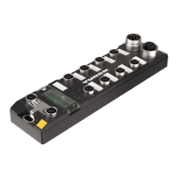
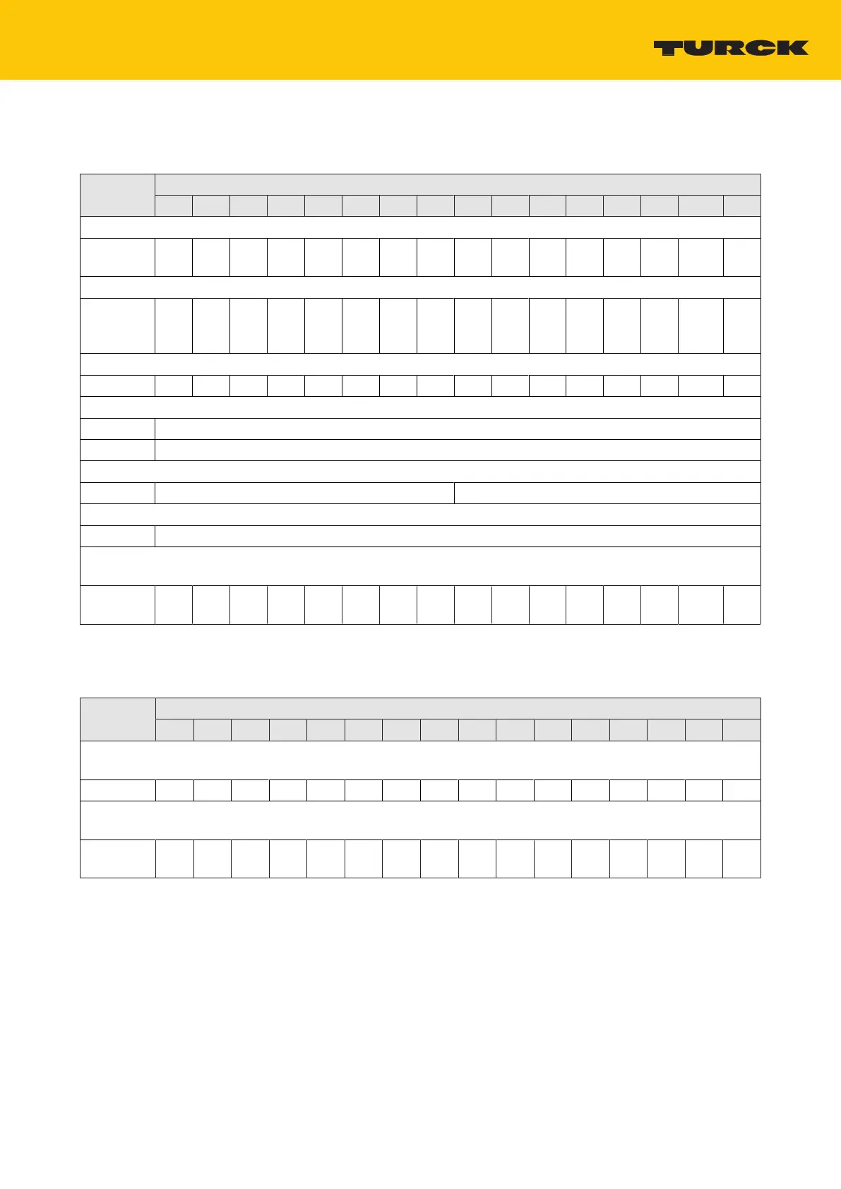
TBEN-S2-8DIP – input registers
Meaning of the process input data [}44]
Register no. Bit no.
15 14 13 12 11 10 9 8 7 6 5 4 3 2 1 0
IN
0x0000 - - - - - - - - DI7
C7P4
DI6
C6P4
DI5
C5P4
DI4
C4P4
DI3
C3P4
DI2
C2P4
DI1
C1P4
DI0
C0P4
Diagn.
0x0001 - - - - - - - - - - - - VERR
V1
C3
VERR
V1
C2
VERR
V1
C1
VERR
V1
C0
Latch IN
0x0002 - - - - - - - - DI7 DI6 DI5 DI4 DI3 DI2 DI1 DI0
CNT Ch0
0x0003 Counter value LSB
0x0004 Counter value MSB
Freq. Ch0
0x0005 Frequency MSB Frequency LSB
Status
0x0006 -
Module
status
0x0007 - FCE - - - COM V1 - - - - - - - ARGEE Diag
Warn
TBEN-S2-8DIP – output registers
Meaning of the process output data [}53]
Register no. Bit no.
15 14 13 12 11 10 9 8 7 6 5 4 3 2 1 0
Latch
reset
0x0800 - - - - - - - - DI7 DI6 DI5 DI4 DI3 DI2 DI1 DI0
Counter
reset
0x0801 - - - - - - - - - - - - - - - CNT
reset
 Loading...