Chapter 2 Operating Principles
2-2.
Operation of Control Parts
2-27 CL-E720DT
+3VIO and +5VIO:
+3VIO and +5VIO are the power supply for driving circuits. Since pin 2 (V3IOON) of the FPGA
is at “High” level and Q26/Q25 and Q24/Q22 turn ON, +3VIO and +5VIO are normally supplied
to the subsequent circuit.
However, in power saving mode, V3IOON goes to “Low” level, and Q26/Q25 and Q24/Q22
turn OFF. Thus, supply of +3VIO and +5VIO stops.
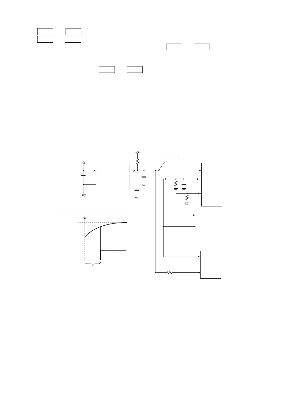
(2) Reset circuit
This circuit performs the system reset.
When power is turned ON, +3.3V gradually increases from 0V. When the voltage at pin 1 (VIN)
of the voltage detector (U2) reaches approx. at 2.8 V, pin 4 (nRST) of U2 changes from “Low”
level to “High” level.
While the nRST signal is “Low”, the CPU (U1A) and the FPGA (U5) are reset.
The CPU outputs the nRSTGA signal to reset the FPGA and other circuits. Also the CPU
outputs the nRSTIF signal to reset the I/F circuits.
VSS
+3.3V
3
2
4
Voltage Detector
nRST
nRST
L : Reset
R1
21_R1
Power ON
Reset
+3.3V
+3.3V
H
L
0V
P3_15
nRSTGA
nRSTGA
P1
21_P1
nRSTV3
nRSTIF
nRST
CPU
U1A
FPGA
U5
R17
R30
(To other circuits)
(To I/F circuits)
R11
U2
XC6119N28ANR-G
OUT
Cd
VIN
1
92
157
C28
[SA Main PCB]
+3.3V
R16
P8-12
64
C26
C27
C47