JHL90 Service Manual
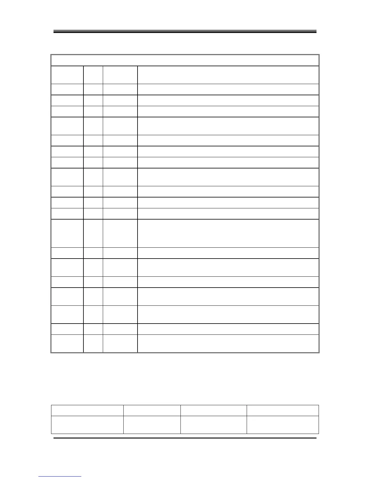
3.10.3 Interface between Power with M/B
DC/DC
Signals I/O Voltage
Level
Description
SUSP# I 0~3.3V Low Active, system suspend control signal
51ON# I 0~floating Low Active, POWER ON control signal.
FSTCHG I 0~3.3V High Active, ENE926 use this pin to control the fast charge of charge
ACOFF I 0~3.3V
High Active, turn off the Adaptor power for battery automatic learning
cycle
ACIN O 0~3.3V High Active, provide to ENE926 to mean the Adaptor power is present
VGATE O 0~3.3V High Active, it will go high when +CPU_CORE is ready
VR_ON I 0~3.3V High Active, turn on/off the +CPU_COREP & VID_VCC
BATT_TEM
P
O 0~3.3V
Analog signal, ENE926 using this voltage level to calculate battery’s
temperature
IREF I 0~3.3V Analog signal, ENE926 using this voltage for setting charge current
VID [0..6] I 0~3.3V The +CPU_CORE voltage depends on those PIN’s VID [6..0]
CHGRTC O 3.3V Charge RTC-battery power source
EC_SMB_
CK1,
EC_SMB_
DA1
I/O 0~5V
Interface of Smbus, communicate between ENE926 and smart battery
SYSON I 0~3.3V High Active, ENE926 use this pin to control the SYSON signal
BATT_OV
P
O 0~3.3V
Analog signal, ENE926 using this voltage level for battery over voltage
protection
PSI# I 0~1.05V Analog signal, enable CPU_CORE regulator at light load mode.
DPRSLPV
R
I 0~1.05V
Analog signal, control CPU C3, C4 signal.
H_DPRST
P#
I 0~1.05V
Analog signal, control CPU C3, C4 signal.
ADP_I I Analog signal, control CPU throttling in UMA SKU
CLK_ENA
BLE#
O 0~3.3V
Analog signal, clock generator enable signal
3.11 BATTERY
3.11.1 Li-Ion smart
3.11.2 Battery Specification
1-1. EE information
6 cell 6 cell 9 cell
Battery Design Capacity
(mAH)
4800 5200 7200
4-10