Appendix B Accessories|VFD-VL
B-27
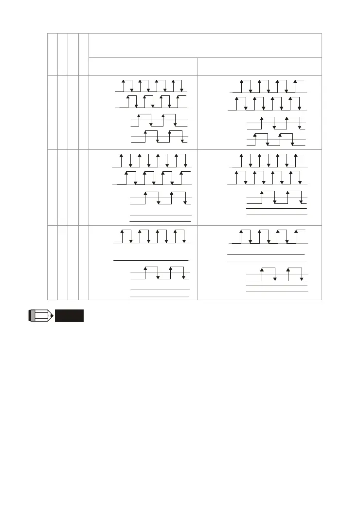
Division factor
RESERVE
I/MODE
O/MODE
RST
A leads B B leads A
X 0 0 1
A-/A
B-/B
A/O-/A/O
B/O-/B/O
A-/A
B-/B
A/O-/A/O
B/O-/B/O
A/O-/A/O
B/O-/B/O
X 0 1 1
A-/A
B-/B
A/O-/A/O
B/O-/B/O
A/O-/A/O
B/O-/B/O
A-/A
B-/B
A/O-/A/O
B/O-/B/O
A/O-/A/O
B/O-/B/O
X 1 X 1
A-/A
B-/B
A/O-/A/O
B/O-/B/O
A/O-/A/O
B/O-/B/O
A-/A
B-/B
A/O-/A/O
B/O-/B/O
A/O-/A/O
B/O-/B/O
NOTE
When the switch is ON, it means logic 0.
A-/A and B-/B are the input signals of PG card. A/O-/A/O and B/O-/B/O are the line
driver outputs of the frequency divider measured by the differential probe.
PIN1 is reserved.
PIN 5~12 are the denominator for the frequency divider. PIN 5 is the low bit (EX: the
setting of XXXX10101010 is that the input signal divides by 85).
When PIN 2 and PIN 3 are set to 0, the input signals (A-/A and B-/B) of PG card
should be square wave and A/O-/A/O and B/O-/B/O are the outputs of frequency
divider.
When PIN 2 is set to 0 and PIN 3 is set to 1, the input signals (A-/A and B-/B) of PG
card should be square wave and B/O-/B/O is the indication of phase A and B. (EX:
Call 1(800)985-6929 for Sales
Call 1(800)985-6929 for Sales
 Loading...