Appendix B Accessories|VFD-VL
B-36
2. Terminals descriptions
Terminal Symbols Descriptions Specifications
VP Power source of encoder
(use SW2 to switch 12V/5V)
Voltage: +5VDC±5% or +8.3 VDC±6%
Current: 250mA max.
0V Power source common for
encoder
Reference level of the power of encoder
A+, A-,
B+, B-
Sine line drive input
(incremental signal)
Input frequency: 40kHz max.
0
0
360 el.
0
90 el.
0
A
B
0.8....1.2Vss
(~
~
1Vss; Z =120 )
0
+SIN, +COS
REFSIN,
REFCOS
Sine line drive input
(incremental signal)
Input frequency: 20kHz max.
REFSIN/REFCOS
0.9...1.1V
SIN
CLOCK+,
CLOCK-
CLOCK line drive output Line Driver RS422 Level output
J3
Data+, Data- RS485 communication interface
Terminal resistor: about 130
TB1
A/O,
A
/O,
B/O,
B
/O
Signal output for PG
feedback card and can be
used as a frequency divider.
Line Driver RS422 Level output
OA
OB
Open collector output signal
and can be used as a
frequency divider
・Transistor open collector output
・Max. 24VDC, 30mA
・VOL≦1.5V(IOL=30mA)
・IOH≦200A(VOH=24VDC)
TB2
GND Open collector output
common
Reference level of NPN transistor open
collector output
J4
Grounding
Connected to the grounding of the power
of the AC motor drive and used for PG
shielding
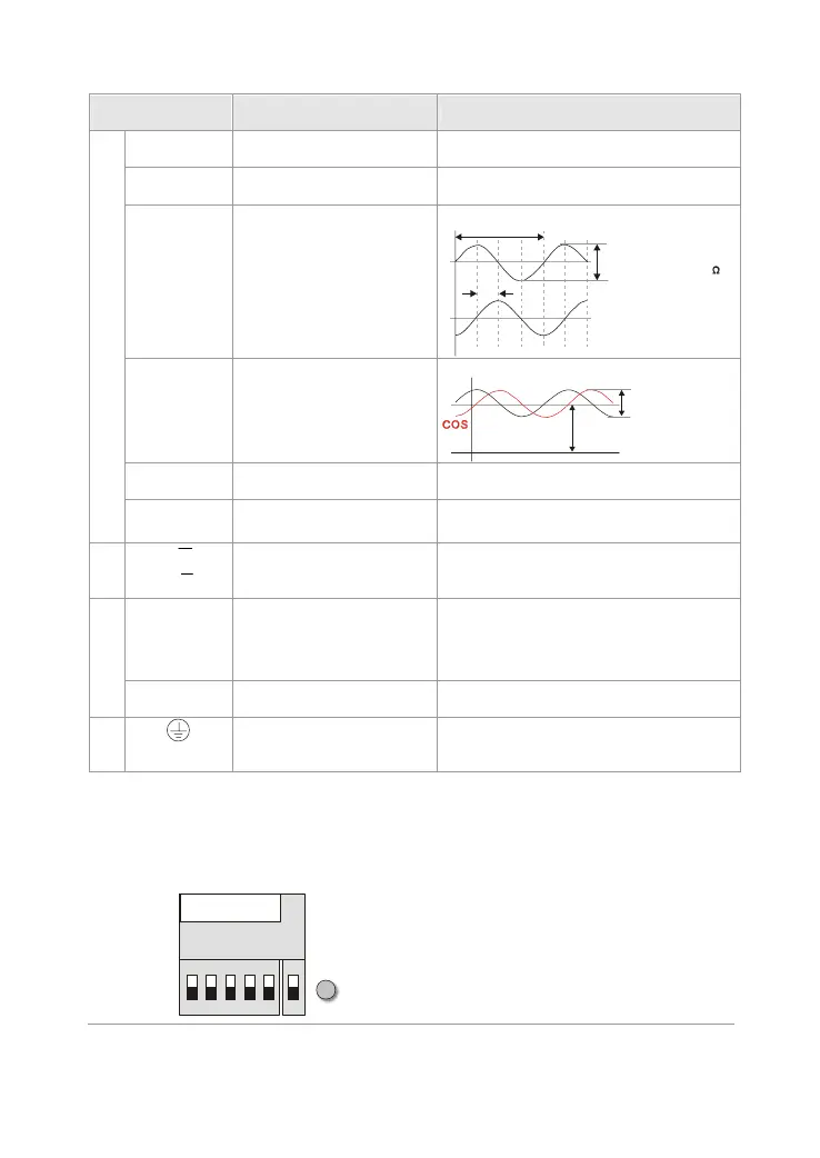
4. Output Signal Setting of the Frequency Divider
It generates the output signal of division factor
“n” after dealing with the input pulse. Please
set by the switch SW1 on the card.
ON
12 3
4
51
RST
Division Factor
BIT0
BIT1
BIT2
BIT3
BIT4
0
1
ON
O/MODE
O/MODE: output type setting of the division
pulse
RST: clock reset bit
Division factor: setting for division factor n:
1~31
Settings and explanations
Call 1(800)985-6929 for Sales
Call 1(800)985-6929 for Sales
 Loading...