Pin Name Module Connector Pins Voltage Description
VCC_MOD 1, 3, 5, 7, 9, 11 3.3 - 5.0 V ±10% Supply for the 1.0 V, 1.35 V/1.5 V and 1.8
V voltage regulators. The input current is
rated at 1.8 A (0.3 A per connector pin).
VCC_3V3 197, 199 3.3 V ±5% Supply for Ethernet PHY, QSPI flash, oscil-
lator, RTC, EEPROM and LEDs
VCC_BAT 200 2.0 - 3.6 V Battery voltage for the RTC and SoC en-
cryption key storage
Table 13: Voltage Supply Inputs
2.10.4 Voltage Supply Outputs
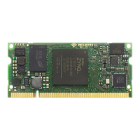
Table 14 presents the supply voltages generated on the Mars ZX3 SoC module, that are available on the
module connector.
Pin Name Module Connector Pins Voltage Maximum Current
9
VCC_1V0 42 1.0 V ±5% 0.3 A
VCC_DDR3L 41 1.35 V/1.5 V ±5% 0.3 A
VCC_1V8 89, 94, 101, 106 1.8 V ±5% 1 A (and max 0.3 A per connector pin)
Table 14: Voltage Supply Outputs
The voltage supply for the DDR3 SDRAM can be set to 1.35 V for low power operation - for details, please
refer to Section 2.14.5.
Warning!
Do not connect any power supply to the voltage supply outputs nor short circuit them to GND, as this
may damage the Mars ZX3 SoC module.
2.10.5 Power Consumption
Please note that the power consumption of any SoC device strongly depends on the application (on the
configured bitstream and I/O activity).
To estimate the power consumption of your design, please use the Xilinx Power Estimator available on the
Xilinx website.
Table 15 lists the power consumption of a Mars ZX3 SoC module, for several applications.
The measurements are based on the reference design using a CPU frequency of 666 MHz, and the DDR3
memory operating in low power mode at 333 MHz.
9
The maximum available output current depends on your SoC design. See sections 2.10.1 and 2.10.5 for details.
D-0000-424-004 22 / 48 Version 05, 21.08.2018

 Loading...