2 Module Description
2.1 Block Diagram
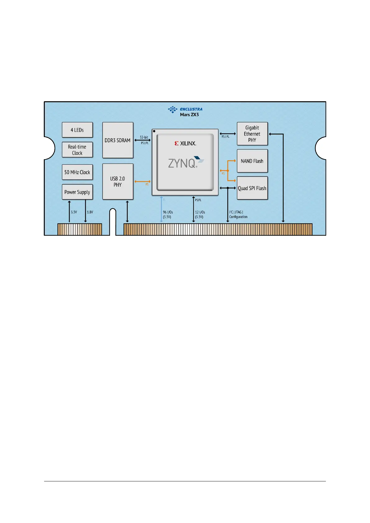
Figure 1: Hardware Block Diagram
The main component of the Mars ZX3 SoC module is the Xilinx Zynq-7000 SoC device. Most of its I/O pins
are connected to the Mars module connector, making 108 user I/Os available to the user.
The SoC device can boot from the on-board QSPI flash, NAND flash or from an external SD card. For de-
velopment purposes, a JTAG interface is connected to Mars module connector.
The available standard configurations include 512 MB NAND flash, a 64 MB quad SPI flash and 512 MB or 1
GB DDR3 SDRAM.
Further, the module is equipped with a Gigabit Ethernet PHY and a USB 2.0 OTG PHY, making it ideal for
communication applications.
A real-time clock is available on the module and is connected to the global I2C bus.
On-board clock generation is based on a 33.33 MHz crystal oscillator.
The module can be operated using a single input supply of 3.3 V DC. All other necessary supply voltages are
generated on-board. Some of these voltages are available on the Mars module connector to supply circuits
on the base board.
Four LEDs are connected to the SoC pins for status signaling.
2.2 Module Configuration and Product Codes
Table 1 describes the available standard module configurations. Custom configurations are available; please
contact Enclustra for further information.
D-0000-424-004 9 / 48 Version 05, 21.08.2018

 Loading...

