2.4 Top and Bottom Views
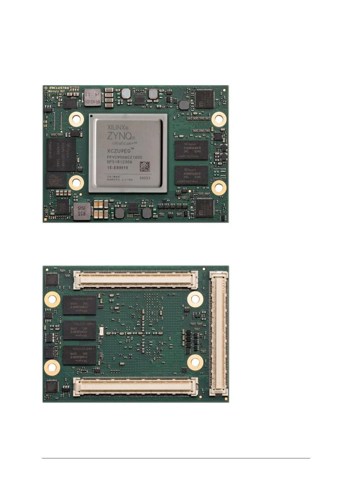
2.4.1 Top View
Figure 5: Module Top View
2.4.2 Bottom View
Figure 6: Module Bottom View
Please note that depending on the hardware revision and configuration, the module may look slightly dif-
ferent than shown in this document.
D-0000-428-001 15 / 66 Version 13, 15.08.2019