In situations in which PCIe functionality is not required, PS_MIO42_PERST# pin can be used in the same
manner as a regular MIO pin.
I/O Pins with Level Shifter
There are four signals on the Mercury+ XU1 SoC module that are routed from the FPGA banks to the module
connector via level shifters - these are presented in Table 7.
I/O Name Module Connector Pin Description
IO_B64_AG4_LS A-88
These pins have a level shifter from VCC_IO_B64
IO_B64_AJ1_LS A-90
to VCC_CFG_MIO
IO_B64_AH11_LS A-92
IO_B64_AG9_LS A-94
Table 7: I/O Pin Exceptions - Level Shifters
The level shifters used for the I/O pins mentioned in Table 7 are NXP NTB0104 and the maximum achievable
data rate on these pins is 40 Mbit/sec. Please note that the level shifter requires the VCC_IO_B64 to be more
or equal to 1.2 V; refer to the level shifter datasheet for details. For VCC_IO_B64 voltages below 1.2 V, the
level shifted signals are not operational.
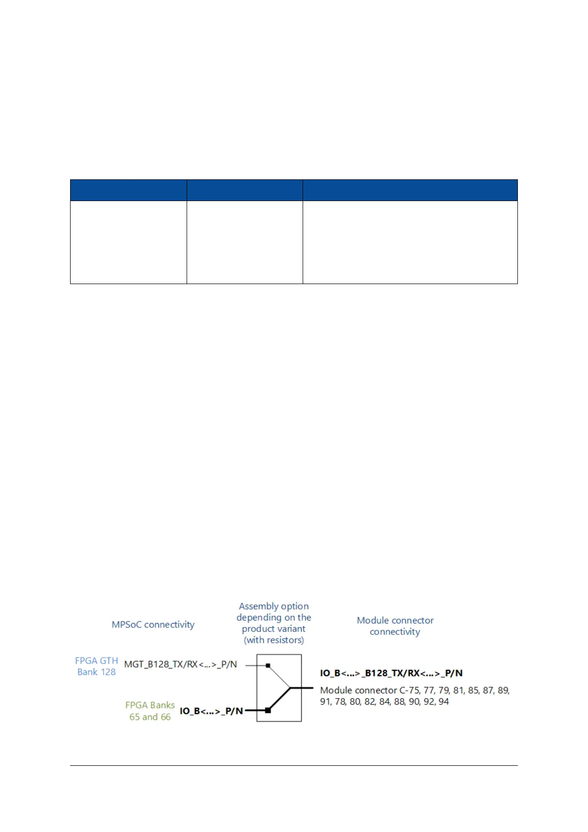
Assembly Options and Migration between Modules
Starting with revision 3 modules, 4 additional GTH transceivers and 2 differential clock pairs may be routed
to the module connector, by using the “G1” assembly variants. This option may be useful when the user
application requires 16 GTH transceivers and less regular I/Os.
Table 8 presents the assembly variants for different product configurations. The signals on the module con-
nector are routed to different types of I/Os, depending on the product variant. To find out where exactly
these pins are routed, refer to the naming conventions for regular user I/Os (Section 2.9.1) and for MGT
signals (Section 2.10). Table 8 is also available in a separate file, FPGA Pinout Assembly Variants Excel Sheet
[5].
Figures 11 and 12 depict the assembly variants information. The default option is marked in bold.
Design support files such as the Mercury Master Pinout [12], Mercury+ XU1 SoC Module User Schematics [6],
and Mercury+ XU1 SoC Module FPGA Pinout Assembly Variants Excel Sheet [5] offer additional information
on assembly options and migration guidelines. In the user schematics, this information is depicted in the
“Assembly Variants” section at the end of the PDF file (MGT_SEL).
Figure 11: Assembly Options for MGT TX/RX Signals
D-0000-428-001 21 / 66 Version 13, 15.08.2019
 Loading...


