2.9.3 Differential I/Os
When using differential pairs, a differential impedance of 100 Ω must be matched on the base board, and
the two nets of a differential pair must have the same length.
The information regarding the length of the signal lines from the MPSoC device to the module connector
is available in Mercury+ XU1 SoC Module IO Net Length Excel Sheet [3]. This enables the user to match the
total length of the differential pairs on the base board if required by the application.
The I/Os in the HD banks (47, 48) can be used only as differential inputs when LVDS/LVPECL standards are
used; LVDS/LVPECL outputs are not supported.
Internal differential termination is not supported for the HD pins; all differential signal pairs from both HD
banks may optionally be equipped with 100 Ω differential termination resistors on the module. Refer to
Section 2.9.6 for details.
2.9.4 I/O Banks
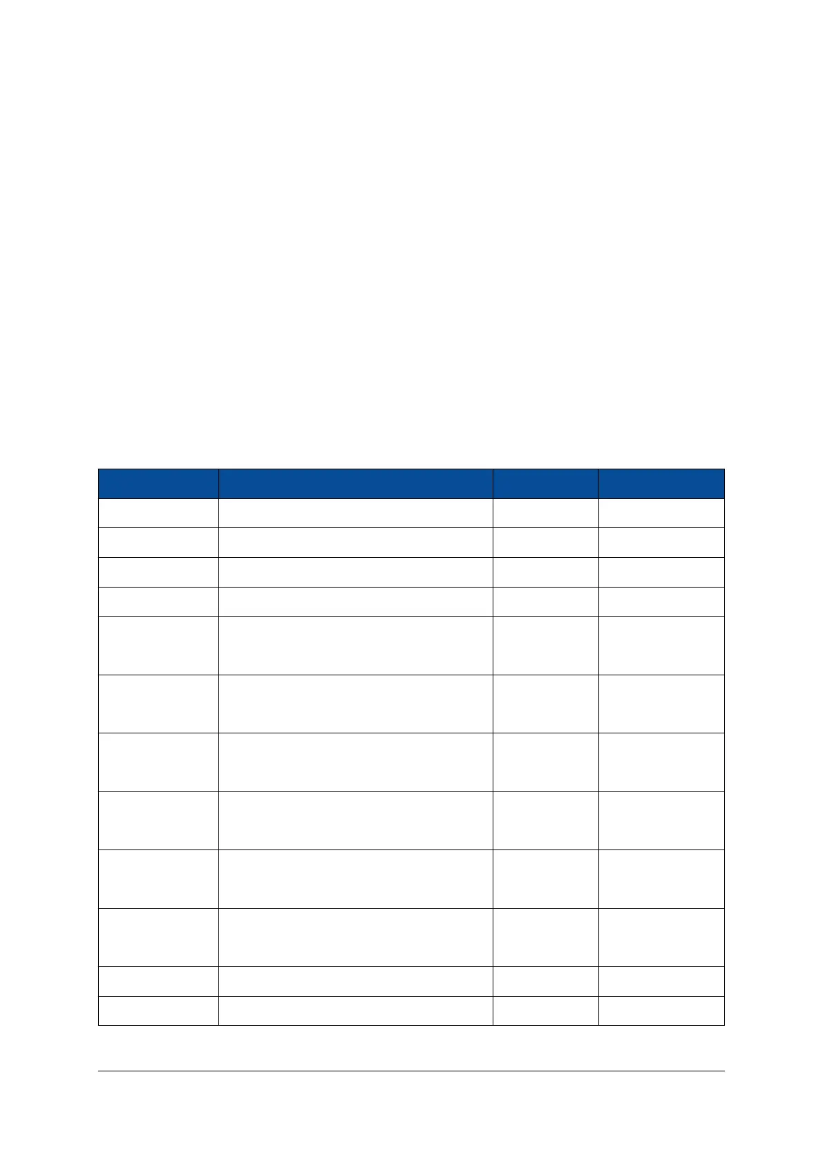
Table 9 describes the main attributes of the Programmable Logic (PL) and Processing System (PS) I/O banks,
and indicates which peripherals are connected to each I/O bank. All I/O pins within a particular I/O bank
must use the same I/O (VCC_IO) and reference (VREF) voltages.
Bank Connectivity VCC_IO VREF
MGT Bank 228 Module connector 0.9 V -
MGT Bank 229 Module connector 0.9 V -
MGT Bank 230 Module connector 0.9 V -
MGT Bank 128
2
Module connector
2
0.9 V -
Bank 64 Module connector
User selectable User selectable
VCC_IO_B64 0.5 × VCC_IO_B64
Bank 65
Module connector
2
User selectable User selectable
VCC_IO_B65 0.5 × VCC_IO_B65
Bank 66
Module connector
2
User selectable User selectable
VCC_IO_B66 0.5 × VCC_IO_B66
Bank 47 Module connector
User selectable
-
VCC_IO_B47
Bank 48 Module connector
User selectable
-
VCC_IO_B48
Bank 503 FPGA PS Configuration
User selectable
-
VCC_CFG_MIO
PS DDR Bank 504 DDR4 SDRAM 1.2 V -
PS Bank 500 eMMC and QSPI flash devices, I2C, LEDs 1.8 V -
Continued on next page...
D-0000-428-001 23 / 66 Version 13, 15.08.2019
 Loading...


