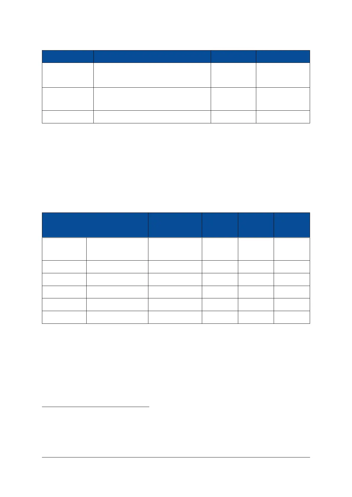
Bank Connectivity VCC_IO VREF
PS Bank 501 Gigabit Ethernet PHY 0, module connector
User selectable
-
VCC_CFG_MIO
PS Bank 502 USB PHY 0, and Gigabit Ethernet PHY 1 / USB
PHY 1 (shared lines)
1.8 V -
PS GTR Bank 505 Module connector, GTR oscillators VCC_0V85 -
Table 9: I/O Banks
2.9.5 VCC_IO Usage
The VCC_IO voltages for the I/O banks located on the module connector are configurable by applying the
required voltage to the VCC_IO_B[x], respectively VCC_CFG_[x] pins. All VCC_IO_B[x] or VCC_CFG_[x] pins of
the same bank must be connected to the same voltage.
For compatibility with other Enclustra Mercury modules, it is recommended to use a single I/O voltage per
module connector.
Signal Name MPSoC Pins Supported Connector Connector Connector
Voltages A Pins B Pins C Pins
VCC_CFG_MIO VCCO_PSIO1_501,
VCCO_PSIO3_503
1.8 V - 3.3 V ±5% 74, 77 - -
VCC_IO_B64 VCCO_64 1.0 V
3
- 1.8 V ±5% - - 76, 116, 158
VCC_IO_B65 VCCO_65 1.0 V - 1.8 V ±5% - 64, 88, 140 -
VCC_IO_B66 VCCO_66 1.0 V
4
- 1.8 V ±5% - 67, 95, 143 -
VCC_IO_B47 VCCO_47 1.2 V - 3.3 V ±5%
5
41 - -
VCC_IO_B48 VCCO_48 1.2 V - 3.3 V ±5%
5
38 - -
Table 10: VCC_IO Pins
3 4 5
If the Mercury+ XU1 SoC module is used in combination with a base board having only two module con-
nectors, the VCC_IO_B64 pin that powers I/O bank 64 is connected to the on-board generated 1.8 V supply
voltage.
2
The MGTs in bank 128 are available on the module connector only on “G1” assembly variants. On these variants, certain I/Os from
banks 65 and 66 are not routed to the module connector. Please check the assembly variants description in Section 2.9.2.
3
There are limitations on the I/Os from bank 64 routed via level shifters when VCC_IO_B64 is less than 1.2 V. Refer to Section 2.9.2
for details.
4
When using voltages lower than 1.8 V for VCC_IO_B66, the I2C bus on FPGA bank 66 is not operational (I2C on PL side is available
starting with revision 2).
5
For voltages of 3.3 V for VCC_IO_B47 and VCC_IO_B48 the tolerance range is -5% to +3%.
D-0000-428-001 24 / 66 Version 13, 15.08.2019
 Loading...


