PCIe Reset Signal (PERST#)
Table 6 lists the I/O pin exceptions on the Mercury+ XU6 SoC module related to the PCIe reset connection.
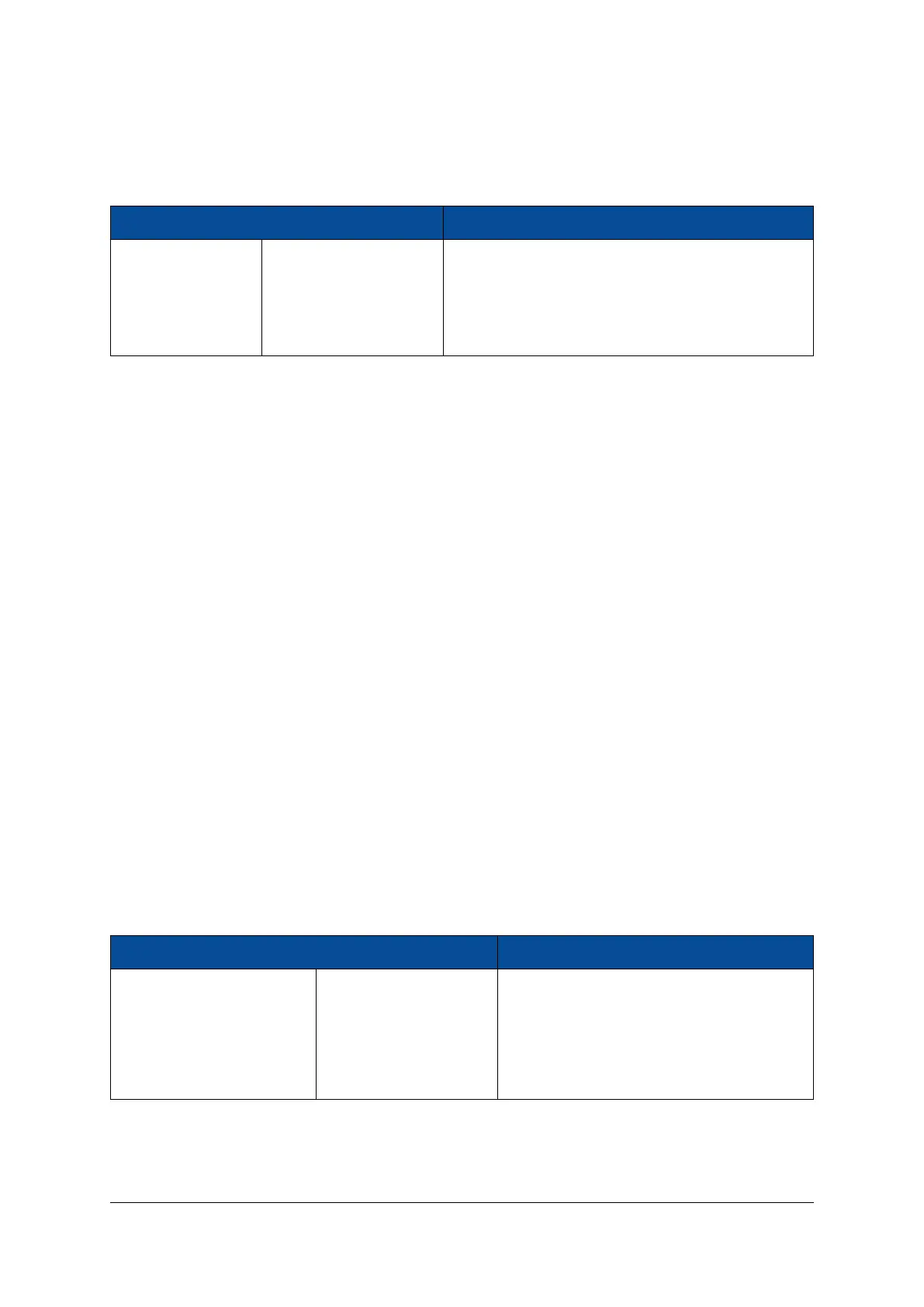
I/O Name Module Connector Pin Description
PS_MIO42_PERST# A-104 When the pin has a low value, its value is routed via a 1
kΩ resistors to ETH_TXD3_PERST# pin (MIO30) and via
a 47 kΩ resistor to IO_B65_L24_PERSTN_H8_N (mod-
ule pin B-126) for PCIe PERST# connection implemen-
tation
Table 6: I/O Pin Exceptions - PERST#
When the Mercury+ XU6 SoC module is used in combination with a Mercury+ PE1 base board as a PCIe
device, the PERST# signal coming from the PCIe edge connector on the module connector pin A-104
(PS_MIO42_PERST#) is driven further to IO_B65_L24_PERSTN_H8_N and to ETH_TXD3_PERST# (MIO30) when
its value is low.
When a PCIe block on the PL side is used, the PERST# signal is connected to the FPGA pin IO_B65_L24_PER-
STN_H8_N via a 47 kΩ resistor. In situations in which a custom board is used or PCIe functionality on the PL
side is not required, this FPGA pin can be used in the same manner as a regular I/O pin.
When a PCIe block on the PS side is used, the PERST# signal is routed via a 1 kΩ resistor to MIO30. This is
the default MIO pin used for the reset signal of the PCIe PS built-in block, therefore it was chosen for the
reset implementation. The Ethernet controller is disabled when the PCIe hard block is used; note that any
other valid position for PERST# would have resulted in having the Ethernet controller disabled.
Using a PCIe block in the PL simultaneously with Gigabit Ethernet interface on the PS side is possible. Si-
multaneous usage of two PCIe endpoints on the PL and PS sides is not supported and was not tested on
Enclustra side.
In situations in which PCIe functionality is not required, PS_MIO42_PERST# pin can be used in the same
manner as a regular MIO pin.
For root complex applications the PERST# signal can be placed on any unused MIO pin (the restriction on
MIO30/42 does not apply in this case).
I/O Pins with Level Shifter
There are four signals on the Mercury+ XU6 SoC module that are routed from the FPGA banks to the module
connector via level shifters - these are presented in Table 7.
I/O Name Module Connector Pin Description
IO_B64_AB5_LS A-88
These pins have a level shifter from VCC_B64
IO_B64_AE4_LS A-90
to VCC_CFG_MIO
IO_B64_AD6_LS A-92
IO_B64_AH6_LS A-94
Table 7: I/O Pin Exceptions - Level Shifters
The level shifters used for the I/O pins mentioned in Table 7 are NXP NTB0104 and the maximum achievable
data rate on these pins is 30 Mbit/sec. Please note that the level shifter requires the VCC_IO_B64 to be more
D-0000-464-001 21 / 58 Version 02, 21.07.2021

 Loading...

