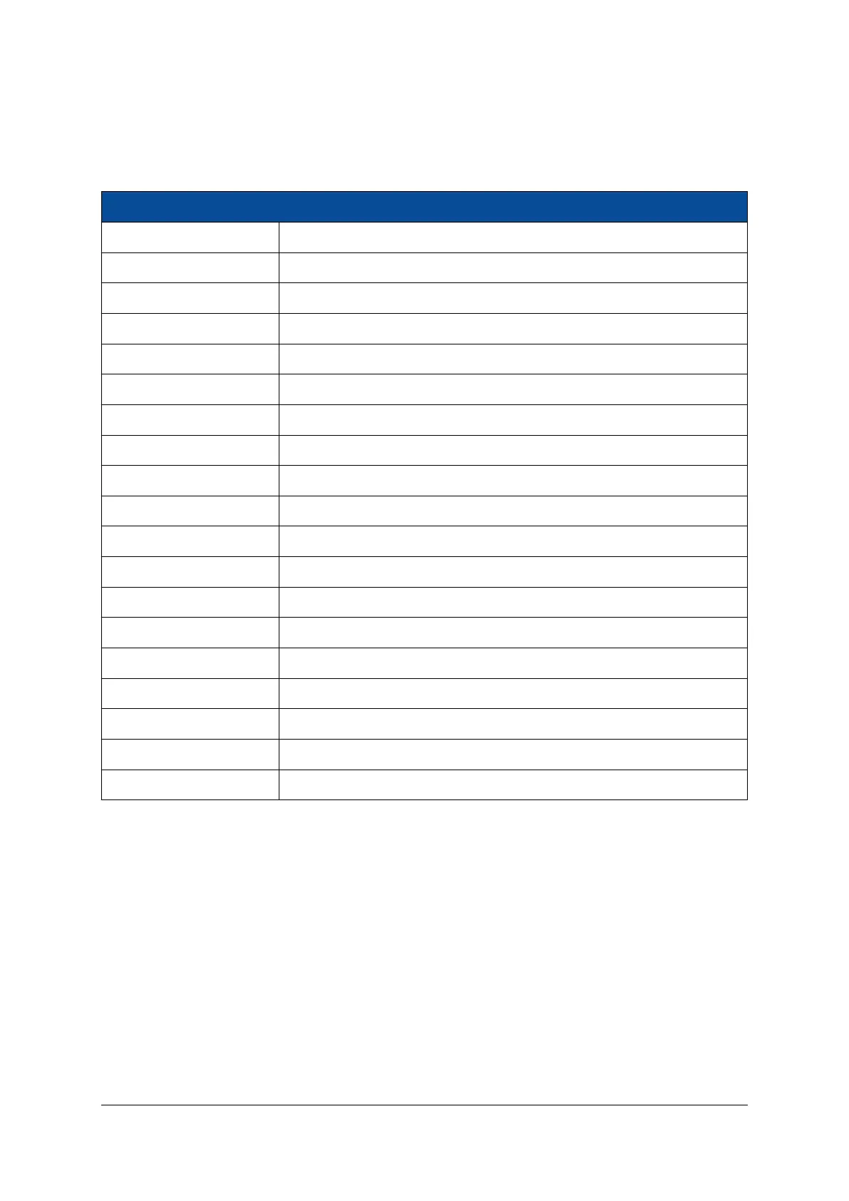
The values given in Table 24 are for reference only. Depending on the equipped memory device on the
Mercury+ XU6 SoC module and on the DDR4 SDRAM frequency, the configuration may be different to the
one in the reference design. Please refer to the memory device datasheet for details.
Parameter Value
Memory type DDR4
DRAM bus width 64 bit (32 bit for ME-XU6-2CG-1E-D10H variant)
ECC Enabled (Disabled for variants without ECC - see Table 1)
DRAM chip bus width 16 bits
DRAM chip capacity 4096-16384 Mbits
Bank group address count 1
Bank address count 2
Row address count 15-17
Column address count 10
Speed bin DDR4 2400T
Operating frequency 1200 MHz
CAS latency 17
CAS write latency 12
Additive latency 0
RAS to CAS delay 17
Precharge time 17
tRC 46.16 ns
tRASmin 32 ns
tFAW 30 ns
Table 24: DDR4 SDRAM (PS) Parameters
2.16 QSPI Flash
The QSPI flash can be used to boot the PS, and to store the FPGA bitstream, ARM application code and
other user data.
2.16.1 QSPI Flash Type
Table 25 describes the memory availability and configuration on the Mercury+ XU6 SoC module.
As there is one QSPI flash chip equipped on the Mercury+ XU6 SoC module, type “single” must be selected
when programming the flash from Vivado tools.
D-0000-464-001 36 / 58 Version 02, 21.07.2021

 Loading...

