CHAPTER 5: SETTINGS GROUPED ELEMENTS
C70 CAPACITOR BANK PROTECTION AND CONTROL SYSTEM – INSTRUCTION MANUAL 5-243
5
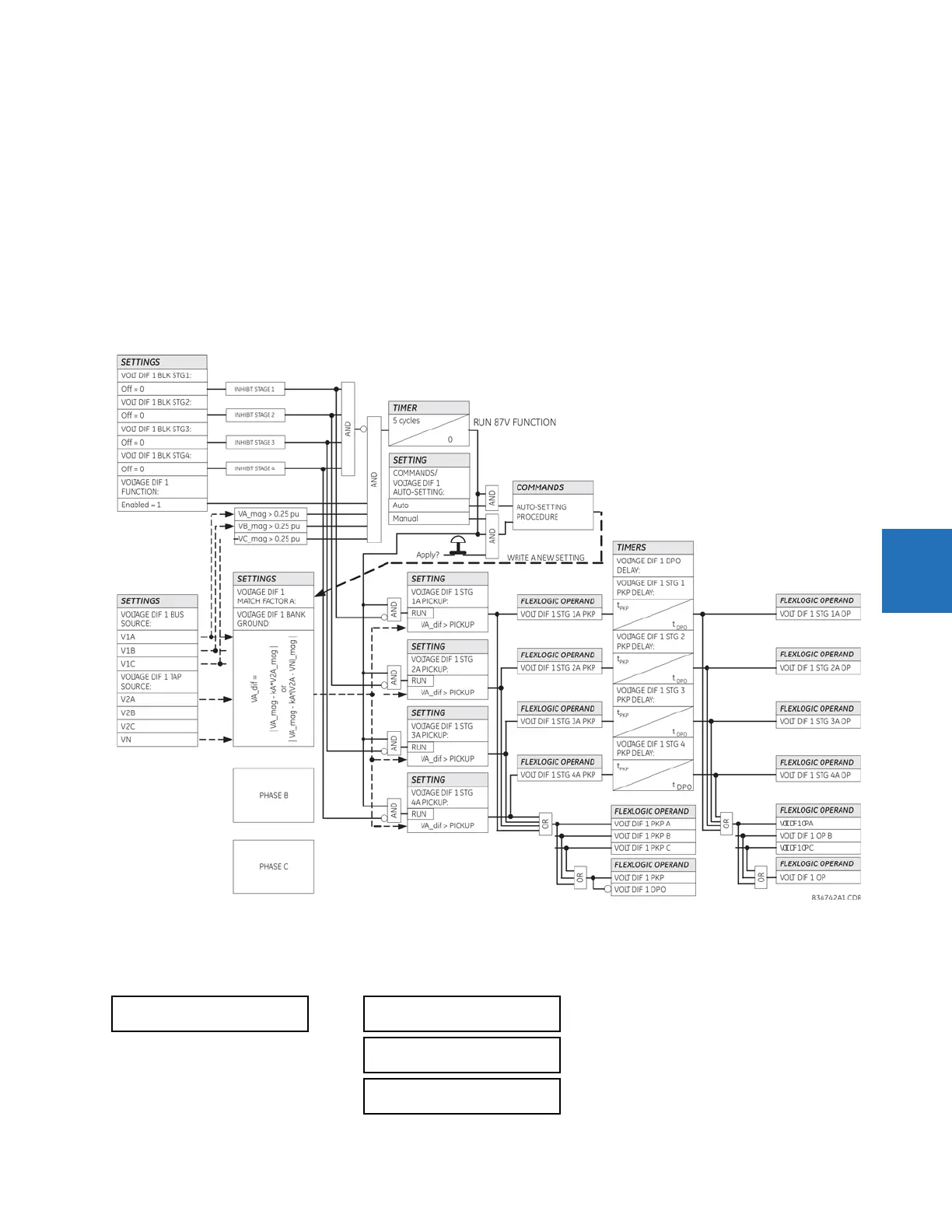
VOLTAGE DIF 1 STG 1 PKP DELAY — Specifies the pickup time delay, individually per each stage of alarming/tripping. Note that
each of the 12 comparators (four stages in three phases) uses an individual timer, but settings for these timers are
controlled individually per each stage, not per phase. The timers use a common drop-out time delay specified by the next
setting.
VOLTAGE DIF 1 DPO DELAY — Controls a drop out delay for the operate FlexLogic operands. Note that individual stages apply
individually configurable pickup delays, but use this common drop out delay.
VOLT DIF 1 BLK STG 1 to VOLT DIF 1 BLK STG 4 — These inputs are used to block the function on a per stage basis when
required. At minimum this function shall be blocked when the bank is offline, or else it operates unnecessarily. Either
breaker position or undercurrent indication via any available instantaneous function, or a combination, can be used for
blocking. Also consider the VT fuse fail condition from both the bus and tap VT. When unblocked, the function becomes
operational after five cycles of intentional delay.
Figure 5-129: Voltage differential logic
5.7.8.8 Bank phase overvoltage (ANSI 59B, IEC PTOV)
SETTINGS GROUPED ELEMENTS SETTING GROUP 1(6) VOLTAGE ELEMENTS BANK OVERVOLTAGE
BANK OVERVOLTAGE 1(3)
BANK OVERVOLTAGE 1
BANK OV 1
FUNCTION: Disabled
Range: Disabled, Enabled
BANK OV 1 BUS
SOURCE: SRC 1
Range: SRC 1, SRC 2, SRC 3, SRC 4, SRC 5, SRC 6
BANK OV 1 NTRL
SOURCE: SRC 1
Range: SRC 1, SRC 2, SRC 3, SRC 4, SRC 5, SRC 6