Home
IEI Technology
Single board computers
WAFER-JL-N5105
IEI Technology WAFER-JL-N5105 User Manual
5
of 1
of 1 rating
79 pages
Give review
Manual
Specs
To Next Page
To Next Page
To Previous Page
To Previous Page
Loading...
W
A
FER-
JL
-N5105 SBC
Page
17
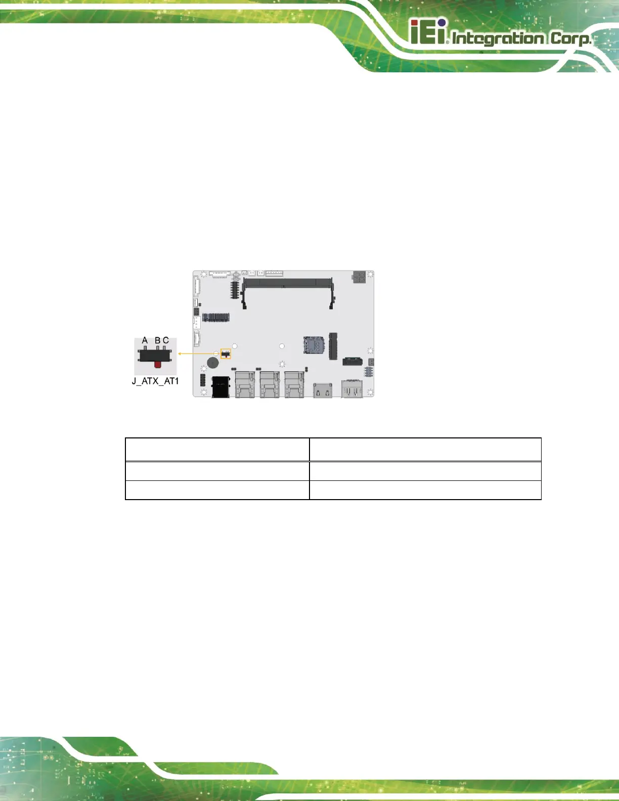
3.2.1
A
T
/A
TX Powe
r M
ode
Setting
CN Label:
J_ATX_
A
T1
CN Type:
3-pin switch
CN Location:
See
787H
Figure
3-3
CN Pinouts:
See T
able 3-4
The
AT/ATX
power m
ode
selection
is
m
ade
throu
gh
th
e
AT
/ATX
power
m
ode
s
witch w
hich
is shown in Figure3
-3.
Figure 3-3:
A
T/
ATX Power M
ode Switch Locations
PIN NO.
DESCRIPTION
Short A - B
A
TX P
ower Mode (de
fault)
Short B
–
C
A
T P
ower Mode
Table 3-4
:
AT/ATX
Power M
ode Switch Pinouts
3.2.2
ME Override Setting Jumper
CN Label:
ME_FL
AS
H1
CN Type:
2-pin header
,P=1.27mm
CN Location:
See
787
H
Figure 3-4
CN Pinouts:
See
T
able 3-5
The
ME_FLAS
H1
connector
is
us
ed
f
or
Flash
Des
criptor
Securit
y
Overid
e
or
ME
Debug
Mode
.
28
30
Table of Contents
Table of Contents
5
Introduction
13
Ntroduction
14
Figure 1-1: WAFER-JL-N5105
14
Features
15
Connectors
15
Figure 1-2: Connectors
15
Dimensions
16
Figure 1-3: Dimensions (MM)
16
Data Flow
17
Figure 1-4: Data Flow Diagram
17
Technical Specifications
18
Table 1-1: Technical Specifications
19
Unpacking
20
Anti-Static Precautions
21
Unpacking Precautions
21
Packing List
22
Table 2-1: Packing List
22
Optional Items
23
Table 2-2: Optional Items
23
Connectors
24
Peripheral Interface Connectors
25
WAFER-JL-N5105 Layout
25
Figure 3-1: Connector and Jumper Locations
25
Table 3-1: Peripheral Interface Connectors
26
External Interface Panel Connectors
27
Internal Peripheral Connectors
27
Clear CMOS Button
27
Table 3-2: Rear Panel Connectors
27
Figure 3-2: Clear CMOS Location
28
Table 3-3: Clear CMOS Pinouts
28
AT/ATX Power Mode Setting
29
ME Override Setting Jumper
29
Figure 3-3: AT/ATX Power Mode Switch Locations
29
Table 3-4: AT/ATX Power Mode Switch Pinouts
29
Figure 3-4: ME Override Setting Jumper Locations
30
Table 3-5: ME Override Setting Jumper Pinouts
30
Audio Connector
31
Figure 3-5: Audio Connector Location
31
Table 3-6: Audio Connector Pinouts
31
ATX 12V Power Connector
32
Digital I/O Connector
32
Figure 3-6: ATX 12V Power Connector Location
32
Table 3-7: ATX 12V Power Connector Pinouts
32
Figure 3-7: Digital I/O Connector Location
33
Table 3-8: Digital I/O Connector Pinouts
33
Fan Connector
34
Figure 3-8: Fan Connector Location
34
Table 3-9: Fan Connector Pinouts
34
Power LED & HDD LED Connector
35
Figure 3-9: Power LED & HDD LED Connector Location
35
Table 3-10: Power LED & HDD LED Connector Pinouts
35
LAN LED Connectors
36
Figure 3-10: LAN LED Connector Locations
36
Table 3-11: LAN1 LED Connector Pinouts
36
Table 3-12: LAN2 LED Connector Pinouts
36
Battery Connector
37
Table 3-13: LAN3 LED Connector Pinouts
37
Figure 3-11: Battery Connector Location
38
Table 3-14: Battery Connector Pinouts
38
Power Button Connector
39
Figure 3-12: Power Button Connector Location
39
Table 3-15: Power Button Connector Pinouts
39
Reset Button Connector
40
Figure 3-13: Reset Button Connector Location
40
Table 3-16: Reset Button Connector Pinouts
40
RS-232 Serial Port Connector
41
Figure 3-14: RS-232 Serial Port Connector Location
41
Table 3-17: RS-232 Serial Port Connector Pinouts
41
SATA 6Gb/S Drive Connector
42
Figure 3-15: SATA 6Gb/S Drive Connectors Location
42
Table 3-18: SATA 6Gb/S Drive Connectors Pinouts
42
SATA Power Connector
43
Figure 3-16: SATA Power Connector Location
43
Table 3-19: SATA Power Connector Pinouts
43
Smbus/I C Connector
44
Figure 3-17: Smbus Connector Location
44
Table 3-20: Smbus Connector Pinouts
44
SPI Flash Connector
45
Figure 3-18: SPI Flash Connector Location
45
Table 3-21: SPI Flash Connector Pinouts
45
USB 2.0 Connector
46
Figure 3-19: USB Connector Location
46
Table 3-22: USB Connector Pinouts
46
Slot, B-Key
47
Figure 3-20: M.2 B Key Slot Location
47
Table 3-23: M. 2 B Key Slot Pinouts
48
Slot, A-Key
49
Figure 3-21: M.2 A-Key Slot Location
49
Table 3-24: M.2 A-Key Slot Pinouts
50
SIM Slot
51
Figure 3-22: SIM Slot Location
51
Table 3-25: SIM Slot Pinouts
51
DDR4 SO-DIMM Socket
52
Figure 3-23: DDR4 SO-DIMM Socket Location
52
External Peripheral Interface Connector Panel
53
Figure 3-24: External Peripheral Interface Connector
53
External 2.5Gbe RJ-45 Connectors
54
Figure 3-25: LAN Location
54
Figure 3-26: LAN LED Location
54
Table 3-26: LAN Pinouts
54
External USB 3.2 Gen 2X1 Type-A
55
Figure 3-27: USB 3.2 Gen 2 Port Location
55
Table 3-27: LAN LED Pinouts
55
External Displayport Connector
56
Table 3-28: USB 3.2 Gen 2 Port Pinouts
56
External Interface Panel Connectors
57
Figure 3-28: External Displayport Connector Location
57
Figure 3-29: HDMI Connector Pinout Locations
57
Installation
58
Anti-Static Precautions
59
Installation Considerations
59
So-DIMM Installation
61
Figure 4-1: SO-DIMM Installation
61
Module Installation
62
Figure 4-2: Inserting the M.2 Module into the Slot at an Angle
62
Figure 4-3: Securing the M.2 Module
62
Chassis Installation
63
Heat Spreader
63
Figure 4-4: Heat Sink Retention Screws
63
Motherboard Installation
64
Figure 4-5: Active Cooling
64
Figure 4-6: Passive Cooling
64
Figure 4-7: DRPC-W-JL-R10
64
Figure 4-8: DRPC-W-JL-R10 with Extra Fan Cooling
64
Internal Peripheral Device Connections
65
AT Power Connection
65
Figure 4-9: Motherboard Installation Example
65
Figure 4-10: Power Cable to Motherboard Connection
66
Channel Audio Kit Installation
67
Figure 4-11: Connect Power Cable to Power Supply
67
RS-232 Cable Connection
68
Figure 4-12: 7.1 Channel Audio Kit
68
SATA Drive Connection
69
Figure 4-13: Single RS-232 Cable Installation
69
Figure 4-14: SATA Drive Cable Connection
70
Software Drivers
71
Available Drivers
72
Driver Download
72
Figure 5-1: IEI Resource Download Center
72
A Regulatory Compliance
74
C Product Disposal
76
D Error Beep Code
78
Pei Beep Codes
79
Dxe Beep Codes
79
Other manuals for IEI Technology WAFER-JL-N5105
Quick Installation Guide
14 pages
5
Based on 1 rating
Ask a question
Give review
Questions and Answers:
Need help?
Do you have a question about the IEI Technology WAFER-JL-N5105 and is the answer not in the manual?
Ask a question
IEI Technology WAFER-JL-N5105 Specifications
General
Brand
IEI Technology
Model
WAFER-JL-N5105
Category
Single board computers
Language
English
 Loading...