160
KEY TIMING PARAMETERS
-6 166 MHz 5.5ns 2ns 1ns
-7 143 MHz 5.5ns 2ns 1ns
-8A 125 MHz 6ns 2ns 1ns
*Off-center parting line
**CL = CAS (READ) latency
SYNCHRONOUS
DRAM
MT48LC1M16A1 S - 512K x 16 x 2 banks
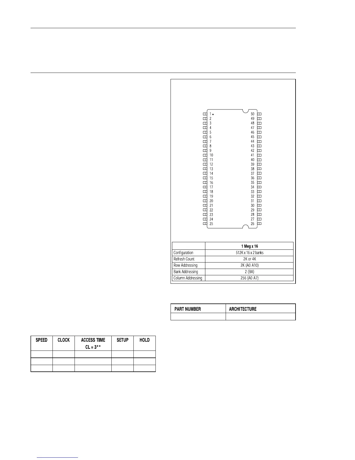
PIN ASSIGNMENT (Top View)
50-Pin TSOP
FEATURES
• PC100 functionality
• Fully synchronous; all signals registered on positive
edge of system clock
• Internal pipelined operation; column address can be
changed every clock cycle
• Internal banks for hiding row access/precharge
1 Meg x 16 - 512K x 16 x 2 banks architecture with
11 row, 8 column addresses per bank
• Programmable burst lengths: 1, 2, 4, 8 or full page
• Auto Precharge Mode, includes CONCURRENT
AUTO PRECHARGE
• Self Refresh and Adaptable Auto Refresh Modes
- 32ms, 2,048-cycle refresh or
- 64ms, 2,048-cycle refresh or
- 64ms, 4,096-cycle refresh
• LVTTL-compatible inputs and outputs
• Single +3.3V ±0.3V power supply
• Supports CAS latency of 1, 2 and 3
OPTIONS MARKING
• Configuration
1 Meg x 16 (512K x 16 x 2 banks) 1M16A1
• Plastic Package - OCPL*
50-pin TSOP (400 mil) TG
• Timing (Cycle Time)
6ns (166 MHz) -6
7ns (143 MHz) -7
8ns (125 MHz) -8A
• Refresh
2K or 4K with Self Refresh Mode at 64ms S
• Part Number Example: MT48LC1M16A1TG-7S
Note: The # symbol indicates signal is active LOW.
V
DD
DQ0
DQ1
VssQ
DQ2
DQ3
V
DD
Q
DQ4
DQ5
VssQ
DQ6
DQ7
V
DD
Q
DQML
WE#
CAS#
RAS#
CS#
BA
A10
A0
A1
A2
A3
V
DD
Vss
DQ15
DQ14
VssQ
DQ13
DQ12
V
DD
Q
DQ11
DQ10
VssQ
DQ9
DQ8
V
DD
Q
NC
DQMH
CLK
CKE
NC
A9
A8
A7
A6
A5
A4
Vss
16Mb (x16) SDRAM PART NUMBER
MT48LC1M16A1TG S 1 Meg x 16
GENERAL DESCRIPTION
The 16Mb SDRAM is a high-speed CMOS, dynamic
random-access memory containing 16,777,216 bits. It is
internally configured as a dual 512K x 16 DRAM with a
synchronous interface (all signals are registered on the
positive edge of the clock signal, CLK). Each of the 512K x
16-bit banks is organized as 2,048 rows by 256 columns by
16 bits. Read and write accesses to the SDRAM are burst
oriented; accesses start at a selected location and continue
for a programmed number of locations in a programmed