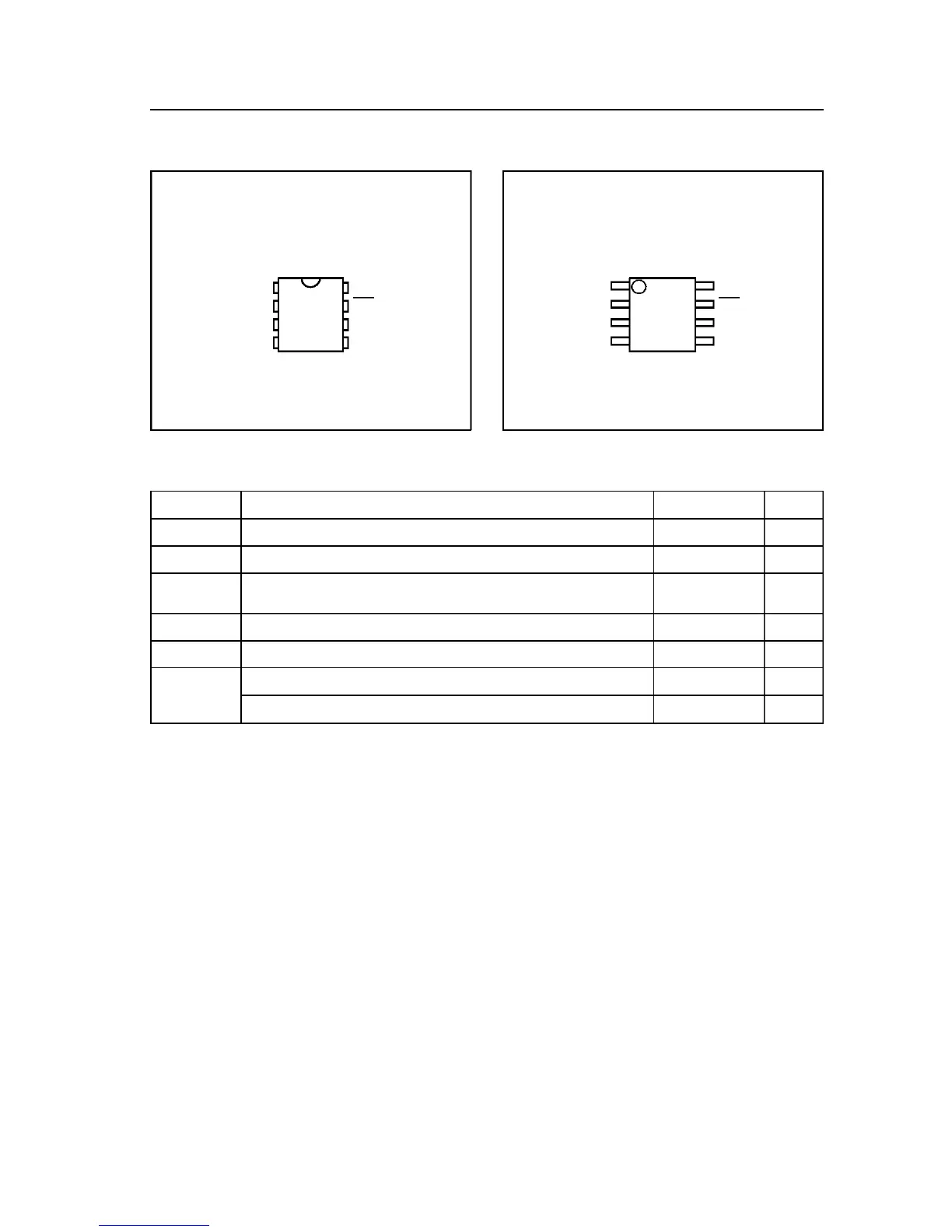
175
SDAV
SS
SCL
WCE1
E0 V
CC
E2
AI01202B
ST24E32
ST25E32
1
2
3
4
8
7
6
5
Figure 2A. DIP Pin Connections
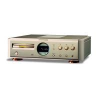
1
AI01203C
2
3
4
8
7
6
5SDAV
SS
SCL
WCE1
E0 V
CC
E2
ST24E32
ST25E32
Figure 2B. SO Pin Connections
Each memory is compatible with the I
2
C extended
addressing standard, two wire serial interface
which uses a bi-directional data bus and serial
clock. The ST24/25E32carry a built-in 4 bit, unique
device identification code (1010) corresponding to
the I
2
C bus definition. The ST24/25E32 behave as
DESCRIPTION (cont'd) slave devices in the I
2
C protocol with all memory
operations synchronized by the serial clock. Read
and write operations are initiated by a START
conditiongenerated by the bus master. TheSTART
condition is followed by a stream of 4 bits (identifi-
cation code 1010), 3 bit Chip Enable input to form
a 7 bit Device Select, plus one read/write bit and
terminatedby an acknowledge bit.
Symbol Parameter Value Unit
T
A
Ambient Operating Temperature ±40 to 125 °C
T
STG
Storage Temperature ±65 to 150 °C
T
LEAD
Lead Temperature, Soldering (SO8)
(PSDIP8)
40 sec
10 sec
215
260
°C
V
IO
Input or Output Voltages ±0.6 to 6.5 V
V
CC
Supply Voltage ±0.3 to 6.5 V
V
ESD
Electrostatic Discharge Voltage (Human Body model)
(2)
4000 V
Electrostatic Discharge Voltage (Machine model)
(3)
500 V
Notes: 1. Except for the rating "Operating Temperature Range", stresses above those listed in the Table "Absolute Maximum Ratings"
may cause permanent damage to the device. These are stress ratings only and operation of the device at these or any other
conditions above thoseindicated in the Operating sections of this specification is not implied. Exposure to Absolute Maximum
Rating conditions for extended periods may affect device reliability. Refer also to the SGS-THOMSON SURE Program and
other relevantquality documents.
2. 100pF through 1500 ; MIL-STD-883C, 3015.7
3. 200pF through 0 ; EIAJ IC-121 (condition C)
Table 2. Absolute Maximum Ratings
(1)
ST24E32, ST25E32