Connectors on Matrox Solios eCL/XCL dual-Base/single-Medium and eCL/XCL-F boards 135
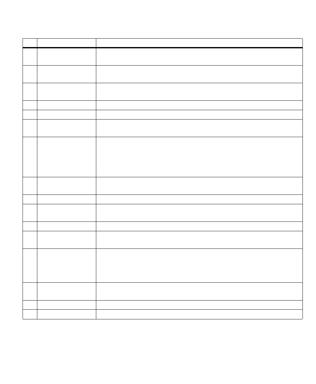
26 P0_LVDS_HSYNC_OUT- HSYNC output for acq. path 0 (negative).
See pin 41 for more information.
27 P0_LVDS_CLK_OUT- Clock output for acq. path 0 (negative).
See pin 11 for more information.
28 LVDS_AUX_IN1- LVDS auxiliary input 1 for an unspecified acq. path (negative).
See pin 12 for more information.
29 GND Ground.
30 GND Ground.
31 LVDS_AUX_IN0- LVDS auxiliary input 0 for an unspecified acq. path (negative).
See pin 32 for more information.
32 LVDS_AUX_IN0+ LVDS auxiliary input 0 for an unspecified acq. path (positive).
Signals only supported for acq. path 0: user-defined input 10.
Signals only supported for acq. path 1: trigger input 0, user-defined input 5, field polarity input, or
quadrature input bit 0.
Signals supported for any acq. path: trigger input 2.
33 P1_LVDS_AUX_OUT0+ LVDS auxiliary output 0 for acq. path 1 (positive).
Supported signals: exposure output 0, user-defined output 5.
34 GND Ground.
35 P1_TTL_AUX_IO_0 TTL auxiliary input/output 0 for acq. path 1.
Supported signals: exposure output 2, trigger input 0, user-defined input/output 2, field input.
36 P1_LVDS_VSYNC_OUT+ VSYNC output for acq. path 1 (positive).
37 P0_LVDS_AUX_IN1+ LVDS auxiliary input 1 for acq. path 0 (positive).
Supported signals: trigger input 1, user-defined input 6, timer clock input, or quadrature input bit 1.
38 OPTO_AUX_IN1+ Opto-isolated auxiliary input 1 for an unspecified acq. path (positive).
Signals only supported for acq. path 0: user-defined input 9.
Signals only supported for acq. path 1: trigger input 1, user-defined input 1.
Signals supported for any acq. path: trigger input 3.
39 OPTO_AUX_IN1- Opto-isolated auxiliary input 1 for an unspecified acq. path (negative).
See pin 38 for more information.
40 P0_LVDS_VSYNC_OUT+ VSYNC output for acq. path 0 (positive).
41 P0_LVDS_HSYNC_OUT+ HSYNC output for acq. path 0 (positive).
Pin Signal Description