138 Appendix B: Technical information
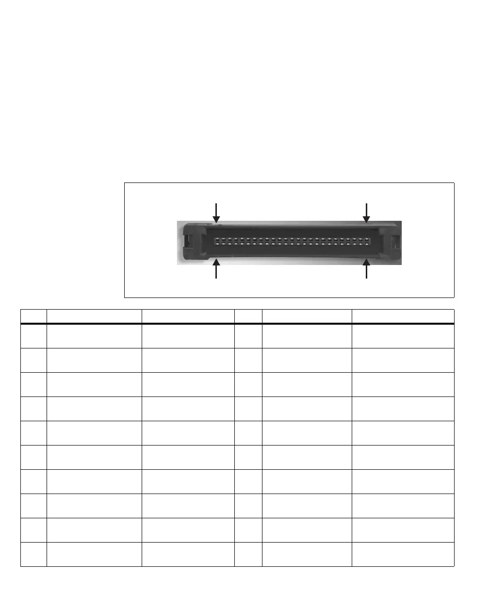
Internal auxiliary I/O connector
The internal auxiliary I/O connector is a 50-pin low-profile IDC connector. It is
used to transmit timing and synchronization signals, and transmit/receive
auxiliary signals. The connector is located on the edge of the board, making the
signals accessible from inside the computer enclosure.
The pinout for this connector is as follows. Refer to the description of the external
auxiliary I/O connectors to establish if an auxiliary signal is specific to an
independent acquisition path and the type of signals that can be routed onto it.
Pin A25
Pin A1
Pin B25
Pin B1
Board side
Pin Signal Description Pin Signal Description
A1 P0_LVDS_HSYNC_OUT+ HSYNC output for acq. path
0 (positive).
B1 P0_LVDS_HSYNC_OUT- HSYNC output for acq. path 0
(negative).
A2 GND Ground. B2 P1_LVDS_HSYNC_OUT- HSYNC output for acq. path 1
(negative).
A3 P1_LVDS_HSYNC_OUT+ HSYNC output for acq. path
1 (positive).
B3 GND Ground.
A4 P0_LVDS_VSYNC_OUT+ VSYNC output for acq. path
0 (positive).
B4 P0_LVDS_VSYNC_OUT- VSYNC output for acq. path 0
(negative).
A5 P1_LVDS_VSYNC_OUT+ VSYNC output for acq. path
1 (positive).
B5 P1_LVDS_VSYNC_OUT- VSYNC output for acq. path 1
(negative).
A6 P0_TTL_AUX_IO_0 TTL auxiliary input/output 0
for acq. path 0.
B6 TTL_AUX_IO_0 TTL auxiliary input/output 0 for
an unspecified acq. path.
A7 P0_TTL_AUX_IO_1 TTL auxiliary input/output 1
for acq. path 0.
B7 GND Ground.
A8 P1_TTL_AUX_IO_0 TTL auxiliary input/output 0
for acq. path 1.
B8 P1_TTL_AUX_IO_1 TTL auxiliary input/output 1 for
acq. path 1.
A9 GND Ground. B9 P0_LVDS_AUX_IN0- LVDS auxiliary input 0 for acq.
path 0 (negative).
A10 P0_LVDS_AUX_IN0+ LVDS auxiliary input 0 for
acq. path 0 (positive).
B10 P0_LVDS_AUX_IN1- LVDS auxiliary input 1 for acq.
path 0 (negative).