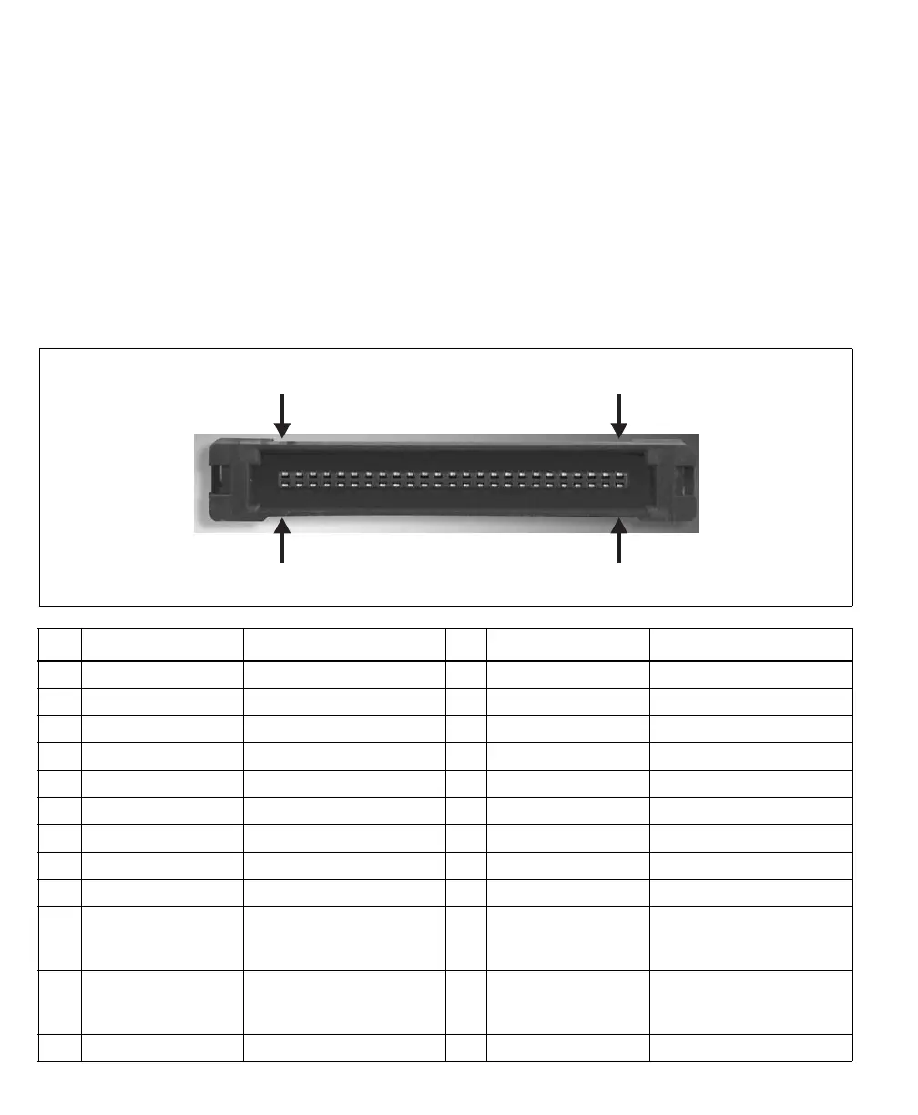
152 Appendix B: Technical information
All the signals are LVTTL signals unless otherwise specified. Note that the clock
and synchronization output signals are the LVTTL version of those output on the
DVI connectors. In addition, you cannot simultaneously receive a clock or
synchronization input signal on this connector and receive the same signal from
the DVI connectors.
The pinout for this connector is as follows. Refer to the description of the external
auxiliary I/O connectors to establish if an auxiliary signal is specific to an
acquisition path and the type of signals that can be routed onto it.
Pin
Signal
1
Description Pin
Signal
1
Description
A1 5 V 5 V power. B1 5 V 5 V power.
A2 GND Ground. B2 P0_LVTTL_CLK_OUT Clock output for acq. path 0.
A3 GND Ground. B3 P0_LVTTL_CLK_IN Clock input for acq. path 0.
A4 GND Ground. B4 P1_LVTTL_CLK_OUT Clock output for acq. path 1.
A5 GND Ground. B5 P1_LVTTL_CLK_IN Clock input for acq. path 1.
A6 GND Ground. B6 P2_LVTTL_CLK_OUT Clock output for acq. path 2.
A7 GND Ground. B7 P2_LVTTL_CLK_IN Clock input for acq. path 2.
A8 GND Ground. B8 P3_LVTTL_CLK_OUT Clock output for acq. path 3.
A9 GND Ground. B9 P3_LVTTL_CLK_IN Clock input for acq. path 3.
A10 P0_LVTTL_AUX(TRIG)_IN Auxiliary input for acq. path 0
(main purpose: trigger 1) from
external auxiliary I/O connector 1.
B10 P1_LVTTL_AUX(TRIG)_IN Auxiliary input for acq. path 1
(main purpose: trigger 1) from
external auxiliary I/O connector 1.
A11 P2_LVTTL_AUX(TRIG)_IN Auxiliary input for acq. path 2
(main purpose: trigger 1) from
external auxiliary I/O connector 1.
B11 P3_LVTTL_AUX(TRIG)_IN Auxiliary input for acq. path 3
(main purpose: trigger 1) from
external auxiliary I/O connector 1.
A12 P0_LVTTL_AUX_OUT0 Auxiliary output 0 for acq. path 0. B12 P0_LVTTL_AUX_OUT1 Auxiliary output 1 for acq. path 0.
Pin A25
Pin A1
Pin B25
Pin B1
Board side