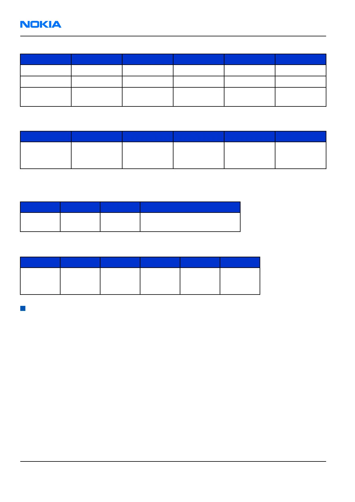
Table 33 Flash LED interface electrical characteristics
Description Parameter Min Typ Max Unit
GPIO28 GPIO output 1.72 1.8 1.92 V
ARMIO4 GPIO output 1.72 1.8 1.92 V
STROBE Strobe signal
output
2 - 2.5 V
Slider switch electrical characteristics
Signal name From To Low value High value Description
GPIO53 Application
processor
S5202 160 mV 1.8 V Slider switch
cover status
signal.
Back-up battery interface connections and electrical characteristics
Table 34 Back-up battery connections
Pin name I/O Connection Notes
L2207,
VBack
-> N2200,
VBack
Back-up battery G2200 is
connected to N2200 via coil
Table 35 Back-up battery electrical characteristics
Description Parameter Min Typ Max Unit
Back-Up
Battery
Voltage
Vback 0 2.5 2.7 V
RF description
Receiver
Introduction to receiver functionality
Receiver functions are implemented in an RF ASIC.
The receiver is a linear direct conversion receiver consisting of separate front ends (LNA (Low Noise Amplifier)
and demodulator) for each supported system. After the demodulators, the signal paths are combined to one
common BB path.
GSM receiver
As GSM Rx branches are functionally identical, the following description is applicable to all of them.
The received signal goes from the GSM antenna to the antenna switch module. The switch module contains
PIN diode switches for a band and Rx/Tx selection and also Rx SAW filters.
The antenna switch module is followed by integrated LNAs (Low Noise Amplifier) residing in an RF ASIC.
The LNAs are followed by demodulators which downconvert the signal to baseband I and Q signals. The
channel select filter is set to 115 kHz.
RM-180
Nokia Customer Care System Module
Page 9 –44 COMPANY CONFIDENTIAL Issue 1
Copyright © 2006 Nokia. All rights reserved.
 Loading...