LPC5411x All information provided in this document is subject to legal disclaimers. © NXP Semiconductors N.V. 2018. All rights reserved.
Product data sheet Rev. 2.1 — 9 May 2018 75 of 105
NXP Semiconductors
LPC5411x
32-bit ARM Cortex-M4/M0+ microcontroller
11.11 USART interface
The actual USART bit rate depends on the delays introduced by the external trace, the
external device, system clock (CCLK), and capacitive loading. Excluding delays
introduced by external device and PCB, the maximum supported bit rate for USART
master synchronous mode is 20 Mbit/s, and the maximum supported bit rate for USART
slave synchronous mode is 16 Mbit/s
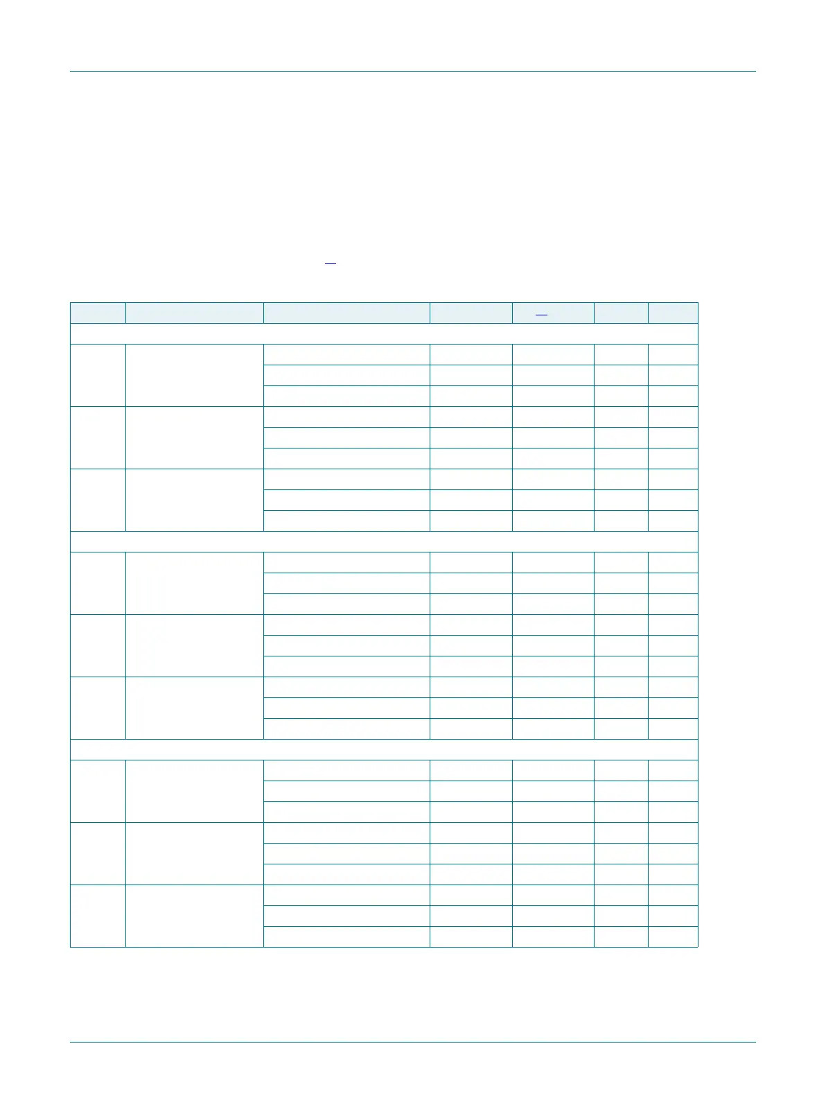
Table 32. USART dynamic characteristics
[1]
T
amb
=
40
C to 105
C; V
DD
= 1.62 V to 3.6 V; C
L
= 30 pF balanced loading on all pins; Input slew = 1 ns, SLEW set to
standard mode for all pins; Parameters sampled at the 90 % and 10 % level of the rising or falling edge.
Symbol Parameter Conditions Min Typ
[2]
Max Unit
USART master (in synchronous mode) 1.62 V V
DD
2.0 V
t
su(D)
data input set-up time CCLK = 1 MHz to 12 MHz 45 - - ns
CCLK = 48 MHz to 60 MHz 39 - - ns
CCLK = 96 MHz 38 - - ns
t
h(D)
data input hold time CCLK = 1 MHz to 12 MHz 0 - - ns
CCLK = 48 MHz to 60 MHz 0 - - ns
CCLK = 96 MHz 0 - - ns
t
v(Q)
data output valid time CCLK = 1 MHz to 12 MHz 2 - 9 ns
CCLK = 48 MHz to 60 MHz 1 - 5 ns
CCLK = 96 MHz 1 - 4 ns
USART slave (in synchronous mode) 1.62 V V
DD
2.0 V
t
su(D)
data input set-up time CCLK = 1 MHz to 12 MHz 1 - - ns
CCLK = 48 MHz to 60 MHz 1 - - ns
CCLK = 96 MHz 1 - - ns
t
h(D)
data input hold time CCLK = 1 MHz to 12 MHz 2 - - ns
CCLK = 48 MHz to 60 MHz 3 - - ns
CCLK = 96 MHz 3 - - ns
t
v(Q)
data output valid time CCLK = 1 MHz to 12 MHz 30 - 55 ns
CCLK = 48 MHz to 60 MHz 23 - 46 ns
CCLK = 96 MHz 22 - 46 ns
USART master (in synchronous mode) 2.7 V V
DD
3.6 V
t
su(D)
data input set-up time CCLK = 1 MHz to 12 MHz 35 - - ns
CCLK = 48 MHz to 60 MHz 27 - - ns
CCLK = 96 MHz 25 - - ns
t
h(D)
data input hold time CCLK = 1 MHz to 12 MHz 0 - - ns
CCLK = 48 MHz to 60 MHz 0 - - ns
CCLK = 96 MHz 0 - - ns
t
v(Q)
data output valid time CCLK = 1 MHz to 12 MHz 2 - 9 ns
CCLK = 48 MHz to 60 MHz 2 - 5 ns
CCLK = 96 MHz 1 - 4 ns
 Loading...


