LPC5411x All information provided in this document is subject to legal disclaimers. © NXP Semiconductors N.V. 2018. All rights reserved.
Product data sheet Rev. 2.1 — 9 May 2018 67 of 105
NXP Semiconductors
LPC5411x
32-bit ARM Cortex-M4/M0+ microcontroller
11.7 Watchdog oscillator
[1] Typical ratings are not guaranteed. The values listed are at nominal supply voltages.
[2] The typical frequency spread over processing and temperature (T
amb
= 40 C to +105 C) is 40 %.
[3] Actual jitter dependent on amplitude and spectrum of substrate noise.
[4] Guaranteed by design. Not tested in production samples.
11.8 I
2
C-bus
[1] Guaranteed by design. Not tested in production.
[2] Parameters are valid over operating temperature range unless otherwise specified. See the I
2
C-bus specification UM10204 for details.
[3] tHD;DAT is the data hold time that is measured from the falling edge of SCL; applies to data in transmission and the acknowledge.
[4] A device must internally provide a hold time of at least 300 ns for the SDA signal (with respect to the V
IH
(min) of the SCL signal) to
bridge the undefined region of the falling edge of SCL.
[5] C
b
= total capacitance of one bus line in pF. If mixed with Hs-mode devices, faster fall times are allowed.
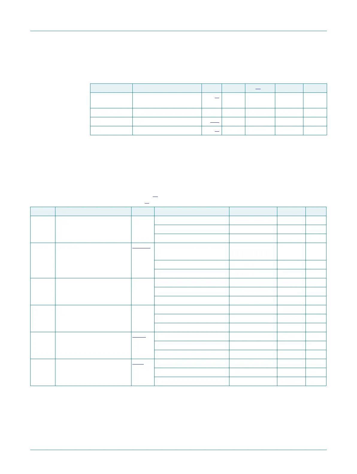
Table 28. Dynamic characteristics: Watchdog oscillator
T
amb
=
40
C to +105
C; 1.62 V
V
DD
3.6 V
Symbol Parameter Min Typ
[1]
Max Unit
f
osc(int)
internal watchdog oscillator
frequency
[2]
6 - 1500 kHz
D
clkout
clkout duty cycle 48 - 52 %
J
PP-CC
peak-peak period jitter
[3][4]
- 1 20 ns
t
start
start-up time
[4]
-4 - s
Table 29. Dynamic characteristic: I
2
C-bus pins
[1]
T
amb
=
40
C to +105
C; 1.62 V
V
DD
3.6 V
[2]
Symbol Parameter Conditions Min Max Unit
f
SCL
SCL clock frequency Standard-mode 0 100 kHz
Fast-mode 0 400 kHz
Fast-mode Plus 0 1 MHz
t
f
fall time
[4][5][6][7]
of both SDA and SCL signals
Standard-mode
- 300 ns
Fast-mode 20 + 0.1 C
b
300 ns
Fast-mode Plus - 120 ns
t
LOW
LOW period of the SCL clock Standard-mode 4.7 - s
Fast-mode 1.3 - s
Fast-mode Plus 0.5 - s
t
HIGH
HIGH period of the SCL clock Standard-mode 4.0 - s
Fast-mode 0.6 - s
Fast-mode Plus 0.26 - s
t
HD;DAT
data hold time
[3][4][8]
Standard-mode 0 - s
Fast-mode 0 - s
Fast-mode Plus 0 - s
t
SU;DAT
data set-up time
[9][10]
Standard-mode 250 - ns
Fast-mode 100 - ns
Fast-mode Plus 50 - ns

 Loading...


